Process knowledge fosters collaboration for cost-effective solutions
SAULIUS MIKALAUSKAS and GEDIMINAS RAČIUKAITIS
Research in laser physics is a strong sector in a knowledge-based economy. Laser science and technology in Lithuania started more than 50 years ago, a few years after the invention of the laser—and training of top-level professionals has been pursued for 40 years. The Lithuanian laser industry has just celebrated its 30th birthday, and laser technologies started to be used in the country around the same time 30 years ago—but the turn to laser microfabrication was made at the beginning of this millennium. Creative and persistent efforts of the people working in the sector have made Lithuanian lasers and laser components desirable goods that are exported to all developed countries. The scientists' publications are widely recognized and well cited, so their contributions stand out in the most prestigious conferences all over the world.
Initial successes
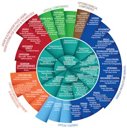
One of the key factors in the success of the Lithuanian laser industry is the permanent and versatile collaboration of the scientists in the research institutions and the engineers of the laser companies, facilitating a dynamic and constantly expanding laser ecosystem (FIGURE 1). This whole community is joined together in the Lithuanian Laser Association.
The products of Lithuania's laser sector are extremely diverse, and include different types of lasers, optics, electronics, mechanical laser components, assemblies, and parts-or combinations thereof. The whole value chain—from the optical component starting with a piece of glass, to advanced optical coatings with multiple dielectric layers deposition, and to mechanics and electronics fabrication—is aligned. This allows companies to produce widely recognized solid-state lasers. Export of these laser products to Japan at the end of the 1990s was a measure of their quality, leading to entry into the markets of other developed countries, the US, and Western Europe.
All the pioneering laser companies and most of the recently founded ones have been established by private initiatives, without foreign investment or direct government support. Initially, they tapped the scientific potential available within Lithuania—whereas currently, the collaboration ties have also been forged with foreign universities. In two decades, the national added value chain has developed, where ideas of new products born in the research labs propagate through the manufacturing chain all the way to the wide network of distributor and service branches all over the globe. Companies and research institutions collaborate in the development of laser technologies, and government and the European Union (EU) encourage new projects. More than 100 different R&D projects were executed in the 2009-2013 funding period.
Laser microfabrication technologies and uses
For the last 15 years, there has been an interest in the industrial application of ultrafast lasers and local companies have increased their production. Laser precision microfabrication became a new goal, searching for real, reliable, and competitive industrial technologies.
Research and industry are collaborating on this new technology, and its uses include:
- Precise machining of micro-components (machinery, the watch industry, and medical stents);
- Selective and high-speed processing of thin films for photovoltaics and electronics, utilizing roll-to-roll (R2R) approaches and working with sensitive materials like copper indium gallium selenide (CIGS);
- Hard materials and ceramics for tooling and electronics;
- Glass and sapphire processing, such as cutting, dicing, and drilling technologies that use conventional Gaussian- and smart-shaped beams;
- 3D processing, such as two-photon polymerization and intra-volume glass processing; and
- Multi-beam processing approaches to enhance productivity and more efficient use of laser energy.
Most of the laser technology-based research is performed at the Department of Laser Technologies of the Center for Physical Sciences and Technology (FTMC) and the Laser Research Center of Vilnius University (both in Vilnius, Lithuania). Their research teams transfer knowledge to companies specializing in technology development, including Workshop of Photonics (WoP; www.wophotonics.com), Evana Technologies, and Femtika (all in Vilnius), and in system integration (ELAS; also in Vilnius), providing next steps by implementation to optical engines and, finally, building laser processing machines. Examples of technologies under development are presented in FIGURE 2.
WoP develops instruments and solutions for ultrafast laser micromachining, specializing in spatially variable waveplates (SVW) embedded in fused silica. SVW fabrication is based on the inscription of self-organized nanogratings inside fused silica using a femtosecond laser. SVWs, which are retardance plates that enable a tailored local control of light polarization, have high damage threshold (up to 20J/cm2)—which is 100 times higher than that of liquid crystal spatial light modulators (0.2J/cm2). Current technology allows fabrication of SVW with retardance from R = 200nm to R = 1000nm in the 400nm to 2μm spectral range. FIGURE 3 shows the International Year of Light 2015 logo and interference color calibration pattern fabricated in fused silica, where various colors appear in cross-polarized light because of destructive interference in the embedded structures.
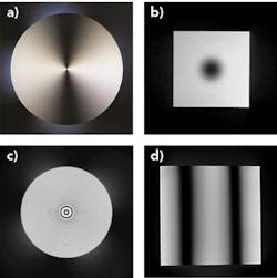
The orientation of induced nanogratings is perpendicular to polarization of the writing laser beam, so it is possible to fabricate predefined slow axis distribution patterns (FIGURE 4). The most common spatially variable waveplates is the S-waveplate, which converts linear polarization to radial or azimuthal polarization. These waveplates have a broad range of applications, from material processing to spin optics in plasmonics.
Evana Technologies (www.evanatech.com), an advanced technology company that provides solutions for laser micromachining and develops scribing technologies for hard materials, has released a compact sapphire scribing engine with advanced double-path scribing features.
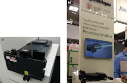
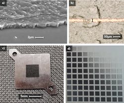
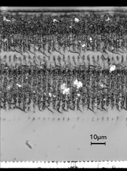
The scribing engine, designed as a single unit (FIGURE 5), consists of a laser (CARBIDE by Light Conversion; also in Vilnius) and an optical module (the FREEZER01, from Evana Technologies). The optical module is tightly attached to the laser, which makes the process more reliable. The laser beam is managed inside the module to produce the desired two-path damage along the cleavage plane of sapphire (FIGURE 6). The damage shape can be optimized to increase the light extraction up to 4% when compared to the standard stealth dicing method. The method provides an opportunity to narrow down (up to ~10μm) the streets on a wafer, with the ability to cleave sapphire wafers up to 300μm thick. The other features of FREEZER01 are finding and tracking the wafer surface with ±2μm precision during the high-speed scribing process (validated at 300mm/s). A new engine incorporates the ICICLE scribing technology (patent pending), which significantly increases light extraction from the LED chip. This is a low-energy-consumption engine that allows processing with power <2W.
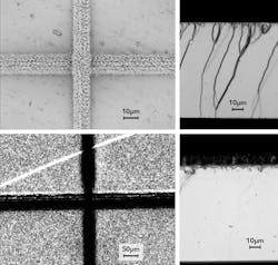
Optical modules dedicated to scribing silicon carbide (SiC) up to 400μm thick use a new technology for uncoated and metal-coated SiC (FIGURE 7).
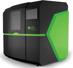
ELAS (www.e-lasers.com) designs and manufactures laser micromachining workstations with ultrafast lasers for scientific and industrial applications. The company, established in 2010, is a spin-off company of FTMC, and is the only company dedicated to the integration of complete laser-based micromachining workstations in the Baltic States, Eastern Europe, and the Nordic countries that are historically in close relationship. Other integrators in the area typically build high-power laser sheet metal cutting or welding systems, so ELAS maintains a strong position in the area as a local supplier of micromachining workstations (FIGURE 8).
Know-how in ultrafast laser development and applications ensure the optimized configuration of laser micromachining equipment to meet process quality and efficiency requirements. Workstations produced by the company are used in eight main application areas that require high-precision material processing:
Cold micro-marking, where long-pulse laser marking can accelerate corrosion of stainless steel-for example, laser marking using ultrafast (picosecond) laser pulses can produce rust-free marking and even enhance resistance to corrosion for some grades of stainless steel, like 316L.
Thin-film solar cell processing, which shows promise for laser scribing of organic photovoltaic (OPV) nanolayers. OPVs offer considerable advantages when compared to conventional silicon-based photovoltaic devices, as they are thin, flexible, lightweight, and can be produced by low-cost, high-yield R2R printing processes. Laser scribing of OPV nanolayers allows for highly integrated modules, with compact series interconnection of the OPV cells.
Flexible electronic manufacturing and selective polymer ablation, as polymers are widely used in diverse fields of everyday life, from household goods to delicate biomedical devices and MEMS. Molding and extrusion are common processes for manufacturing parts from polymers. Excimer lasers are usually used for processing polymers related to the mask technique. Because of excimer lasers' specific features, there is an overall tendency to replace them by solid-state lasers for laser-direct writing. This technique offers flexibility, which is especially important at the development stage of micro-devices.
Silicon, glass, and sapphire wafer cutting and scribing, where using laser technology for manufacturing these photonic components is a very important achievement. One area is dicing of light-emitting diodes (LEDs) grown on sapphire substrate for singulation. Sapphire is mechanically and chemically difficult to machine. An ELAS-patented technology relates to cutting of transparent materials based on the use of radiation from an ultrafast laser with two wavelengths, and their temporal and/or spatial alignment. Optimized micromachining parameters allowed achieving high-quality scribing line and increasing the process speed.
Metal, synthetic diamond, or ceramic mechanical tools treatment, since laser processing of composite materials, as well as cutting-edge generation technology based on ultrafast pulses, has drawn a lot of attention in the past few years. Processing of ultra-hard materials such as polycrystalline diamond, natural diamond, tungsten carbide, and CERMET with picosecond pulses provides a new opportunity. The key parameters that are critical for industrial applications are the processing time and processing quality.
Medical device manufacturing, where laser micro-processing is a technology that enables fabrication of components with micrometer accuracy. For applications such as stent therapy (especially in coronary heart disease), catheters, intraocular lenses (IOLs), vascular clips, and surgical staples, the highest micro-material processing quality is necessary. Laser micromachining provides extremely gentle processing that has led to continuous growth in this industry. The ultrafast, high-energy laser pulses allow material processing without a heat-affected zone (HAZ) or burr formation. Multi-axis and multi-wavelength options allow arbitrary geometries and a variety of materials.
Optical and metal coatings patterning, as the flat-panel display and photovoltaic industries challenge the development of new laser technologies. Patterning of thin films on various substrates is important in the booming market for liquid-crystal display (LCD) and organic LED (OLED) displays, and large investments into photovoltaics. Picosecond lasers are used in processing of a variety of thin films and multi-layers on rigid and flexible substrates.
Fuel-injector nozzle drilling with laser-based machines is an attractive alternative to other methods, as ultrafast lasers are being used to drill or cut through the material with the laser beam concentrated precisely on the working area. As a result, evaporation of the material takes place without the melting phase and any further burr removal is not necessary. Parameters such as high-accuracy drilling, processing speed, and flexible hole shaping make laser micromachining technology the best choice for fuel-injector nozzle production.
Conclusion
Deep process knowledge from local partners, as well as the collaboration with the Department of Laser Technology at FTMC, allows development and building workstations tailored to specific applications that are also optimal and cost-effective solutions that meet industrial standards.
SAULIUS MIKALAUSKAS([email protected]) is with ELAS and GEDIMINAS RAČIUKAITIS([email protected]) is with FTMC and EKSPLA, all in Vilnius, Lithuania.
