Pico- and femtosecond lasers work in chemical and physical processing of graphene
IVAN BOBRINETSKIY and PABLO ROMERO
Ultrafast lasers (picosecond and femtosecond) are extensively used in thin film patterning in the development and fabrication of micro- and nanoelectronic devices, including photovoltaics, displays, sensors, or large-area organic electronics. The main advantages of ultrafast lasers are related to the limited thermal effects and fast energy dissipation, allowing patterning of ultrathin films in complex multi-layered structures.
The upcoming era of nanomaterials brings new possibilities for extremely fast, efficient, and miniaturized devices. But processing these new nanomaterials, down to the single atomic layer, offers challenging technological difficulties. This article describes the application of ultrafast laser patterning to the atomic-scale, two-dimensional carbon lattice-namely graphene.
Graphene and laser irradiation
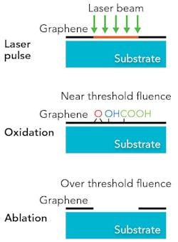
Graphene has attracted enormous interest over the last decade, owing to its unique properties that make it attractive for a wide variety of applications, including photonics, optoelectronics, sensors, chemical reactions, and energy storage, among others [1]. Different processing techniques have been developed for graphene-based technology, mainly based on conventional methods from silicon microelectronics. Laser processing is just starting to be used in graphene device development, but is starting to show huge potential. Laser beams can be used for various types of graphene treatment, including laser-assisted graphene growth (LIG, from silicon carbide and polyimide), patterned ablation on different substrates, and even in chemical modification (oxidation and functionalization; FIGURE 1). These can be used for direct integration in different optoelectronic, photonic, and nanoelectromechanical systems (NEMS) devices.
Ultrafast lasers can replace multistep photolithography with a single step, direct-write laser process [2], where it is critical and beneficial for graphene to avoid any impurities on its surface from wet processing.
Patterned ablation of graphene
While only one or a few atomic monolayers in thickness, the optical absorption of graphene is relatively high in a wide window of the electromagnetic spectrum. For single-layer suspended graphene, this value was precisely measured to be 2.3% for visible light. Moreover, graphene on a substrate can provide even 10 times higher absorption, depending on the substrate nature and the interface. When using ultrafast lasers with very high photon density, the absorption can be further enhanced.
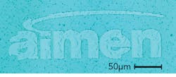
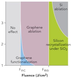
This provides the possibility of accurate and efficient graphene ablation (FIGURE 2). Electronic applications normally require graphene to be placed on thermally grown silicon oxide on silicon substrate. The highly efficient absorption of graphene in this configuration results in graphene ablation without damage to the silicon or silicon oxide (FIGURE 3).
Because of the atomic-scale thickness of graphene, it is possible to use a single-shot ablation regime that will decrease the total processing time. Feature sizes of 1μm or less can be achieved, and sub-wavelength resolutions can be achieved using laser-induced multiphoton processing.
Photochemistry of graphene
Photochemical processing of material surfaces is a well-known process, where—under light irradiation (typically UV)—material properties are changed by the internal phase transition or chemical reaction with surrounding environment (gas, vapors, and liquids). The most popular application of photochemistry in laser processing is for additive manufacturing procedures based on multiphoton polymerization using laser irradiation. This provides a unique processing tool in 3D chemical processing of polymer and composite materials. The same holds for carbon-based graphene, which can also be chemically modified by strong UV oxidation.
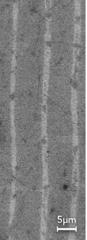
Graphene is a unique material for both its electronic and optical properties. Nonlinear optical effects are verified in graphene, such as multiphoton absorption, plasmon generation (a plasmon is a collective excitation of the electronic "fluid" in a piece of conducting material), Q-switching, etc. By exploiting these nonlinear optical effects, it is possible to change chemical and optical properties of graphene with high-intensity visible light. The typical reaction of graphene in oxygen/water atmosphere with a 515nm ultrafast laser results in local oxidation of graphene (FIGURE 4).
The result is the ability to generate freeform structures (maskless) with sub-micron resolution, at high processing speeds (up to several meters per second using conventional optical scanners), and with extreme property switch and contrast in conductivity, light manipulation, and surface properties, like wettability. This is a powerful result, as it allows the rapid development of a wide variety of devices for biology, security, or communications.
The variety of technological properties of graphene is far beyond the traditional solid-state material currently used in electronics, microelectromechanical systems (MEMS), and micro-opto-electromechanical systems (MOEMS). These new properties are still being discovered, and making use of laser processing can provide scalable, fast, reproducible, and impurity-free technology for the integration of graphene in the new microelectronics platform.
ACKNOWLEDGEMENTS
The authors acknowledge the European Union's Seventh Framework Program for research and technological development (Grant Agreement No. 316161).
REFERENCES
1. A. C. Ferrari et al., Nanoscale, 7, 4598–4810 (2015).
2. I. I. Bobrinetskiy, A. V. Emelianov, N. Otero, and P. M. Romero, Appl. Phys. Lett., 107, 043104 (2015).
IVAN BOBRINETSKIY ([email protected]) is research scientist and PABLO ROMERO ([email protected]) is Research Strategy Manager at AIMEN Laser Application Center, O Porriño, Pontevedra, Spain; www.aimen.es.


