Process and laser optimization are key for high throughput and precise clean scribes
Arecent article presented an overview of how lasers can play a key role in the development and production of solar devices, delivering twin benefits of lower fabrication costs and superior performance (see ILS, August 2007, p. 24). Laser scribing is rapidly emerging as one of the most significant of all these processes as it is critically enabling high-volume production of next-generation thin-film devices, surpassing mechanical scribing methods in quality, speed, and reliability.
These thin-film solar cells are important because they lend themselves to streamlined, high-volume manufacturing and greatly reduced silicon consumption. This results in dramatically lower fabrication costs per unit of power output compared to traditional silicon-wafer-based solar cells.
Fabrication steps
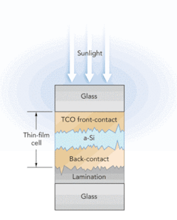
As implied by their name, “thin-film” devices typically consist of multiple thin layers of material deposited on sheet glass. While other formats and materials are at early stages of development, initial volume production of thin-film solar cells is being dominated by devices based on amorphous silicon (a-Si) in a so-called single-junction configuration (see Fig. 1). Multijunction a-Si variants such as the tandem ‘micromorph’ structure are expected to follow soon. But the laser-scribing processes described here are applicable to all other thin-film systems under development, including those based on CdTe (cadmium telluride) and cigs (copper indium gallium selenide).
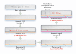
It’s important to understand that these are large panels; the current industry-standard dimensions are 1100 × 1300 mm, and the next generation will be 2200 × 2600 mm. These glass panels are typically subdivided into a large number (between 100 and 200) of individual solar cells by scribing processes that also define the electrical interconnects for adjacent cells (see Fig. 2). This scribing creates low-current active ‘strips,’ typically only 5-10 mm wide, which are electrically connected in series to produce high power (from tens of watts to a couple hundred watts, typically) with currents of a few amps.
FIGURE 2. After each of the different material thin films are deposited, the film must be patterned using narrow scribes to create a series of thin strip-shaped solar cells.
Each panel starts off as a sheet of glass with a typical thickness of 3 mm. This is called a glass superstrate, because sunlight will enter through this support glass. The first step is to deposit a continuous, uniform layer of tco (transparent conductive oxide) with a typical thickness of a few hundred nanometers, which will form the front electrodes. This is followed by a scribe process called P1, which scribes through the entire layer thickness. The next step is vapor deposition of p- and n-type silicon with a total thickness of 2-3 µm, again followed by a scribing step, called P2, which completely cuts through the silicon layer. The final deposition is the thin (submicron) metal (Al or Mo) layer that forms the rear electrodes. These are patterned using a third scribe process, called P3. The panel is then sealed with a rear surface glass lamination.
Scribing requirements
To attain economic viability, thin-film devices must be produced in high volumes for low unit costs. Fast process throughput (short takt times) is critical to minimizing scribing costs. But high-quality scribes with very low defect counts are also necessary to deliver a high yield of final product with the highest possible electrical-conversion efficiency.
As with many other laser micromachining applications, both resolution and precision are important. Specifically, the area between P1 and P3 is a nonactive (that is, wasted or ‘dead’) area. Scribe lines are currently on the order of several tens of microns in width, with an offset separation between P1 and P3 of tens to hundreds of microns. But given that each cell has a total width of less than 10 mm, together with the importance of maximizing the inherently low conversion efficiency (6%-10% versus 15%-20% for bulk Si devices), it is vital to further minimize this already small scribe area. That means narrow scribes that are placed as close to each other as possible, with minimum offset. (Next-generation product is projected to use line widths in the 25-30-µm range.) The use of more closely spaced scribes requires very straight cuts that don’t wander out of alignment. Scribe narrowing also must be accomplished without increasing scribe defects.
Cut quality in terms of edge roughness and layer peeling is another important consideration, because solar conversion efficiency is substantially reduced by microcracks, and other types of surface and subsurface thermal damage. Therefore, it is vital to create scribes with a minimal haz (heat affect zone), smooth edges, and no recast debris.
However, this application is somewhat unique in that it must combine this precision, resolution, and edge quality with very high speed. Panels are produced in a continuous-flow production line. The typical amount of time a panel spends in a specific process step is widely considered to be in the range of only a few tens of seconds for small panels and a few minutes for larger sized panels. Yet each panel requires literally hundreds of meters of scribing. Even in workstations that utilize several lasers, scribe rates have to be in the range of 2 m/s, and each scribe has to be accomplished in a single pass. Moreover, active depth control is not realistic-each laser scribe depth must be naturally limited by material selectivity.
This does not represent a significant obstacle for the P1 scribe, which only needs to remove a few hundred nanometers of tco. Although quite demanding on certain laser parameters, it can be performed using conventional techniques with the near-infrared (1.06 µm) output of a Q‑switched dpss (diode-pumped solid-state) laser. But the P2 and P3 scribes must remove a few microns of thickness of silicon, plus the overlaying metal film in the case of P3. Conventional (thermal) materials processing cannot deliver the combination of single-pass speed, as well as cut quality and spatial resolution. Photoablation with a fast-pulsed UV laser is not an option, as this application would not sustain the cost of the laser and, more important, such a laser would provide no material selectivity and, hence, depth control: it would ablate all the materials and could damage the glass.
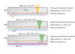
The solution is a laser lift-off process that has been developed in different forms for other applications. Instead of melting, vaporizing, or atomizing all the target material, this lift-off process vaporizes a small amount of material at the film interface, removing the overlaying layers entirely in a microexplosive effect. This is the principal reason that these scribes are performed through the glass (see Fig. 3). Specifically, P2 and P3 scribes are accomplished using a fast-pulsed green (532 nm) dpss laser.
Figure 3. P1 is performed using a focused near-infrared laser to remove the TCO. P2 and P3 rely on selective absorption of a green laser at the TCO-Si interface, removing the Si through a microexplosive lift-off process.
Both the glass and tco are transparent at this wavelength which is strongly absorbed by the Si. So the entire laser pulse energy is trapped at the interface enabling the Si to be completely lifted in a single pass. P2 and P3 use a masked (circular aperture) beam, rather than a focused Gaussian beam as in P1. The relatively low thermal conductivity of silicon means that this fast process leaves clean edges, as defined by the laser mask edges, and does not cause thermal damage to the surrounding silicon.
Laser optimization
The unique economic aspects of solar-panel scribing require a very specific set of laser parameters for process optimization. Coherent has developed a family of near-infrared and green prisma lasers optimized to meet these critical parameters.
Power requirements are actually fairly modest because the limiting speed of the scan optics dictates the use of multiple lasers in parallel. P1 uses lasers with up to 8 W of near-IR. But the P2 and P3 steps only need a few hundred milliwatts of green output. A much more critical requirement is pulse-repetition rate; with a target scan rate of 2 m/s for the largest panels, the pulse-repetition rate has to be very high (up to 100 kHz or higher) to achieve the desired scalloped profile (see Fig. 4).
These new scribing lasers have also been designed to deliver high pulse-to-pulse energy stability and extreme pointing stability. The energy stability is necessary to obtain the required scribe consistency. And the pointing stability (<50 µrad) supports narrower scribe lines, with closer spacing planned for next-generation panels. This pointing stability is particularly critical because these larger panels involve longer beam-delivery paths than ever before in this application, amplifying any drifts in beam-pointing direction.
Reliability, up-time, and serviceability are other critical laser characteristics, given that a production line involves three separate scribing stations, each using multiple lasers. If any single laser malfunctions in any way, the entire line must be stopped. And, finally, minimized and predictable maintenance downtime is a closely related need.
Solar-cell manufacturing is a demanding application for lasers because it requires high precision and yet is also extremely cost-sensitive. This challenge can only be met by utilizing a laser whose output has been specifically optimized for the needs of this high-speed process and which has been designed and constructed to deliver a very high level of operational consistency and reliability.
Corey M. Dunsky, [email protected], and Finlay Colville, [email protected], are with Coherent Inc.; www.coherent.com.


