Tuan A. Mai
Several unsophisticated techniques are available to help laser users achieve debris-free machining
The characteristic noncontact and the much-localized heat input from a finely focused beam have made the laser a perfect choice for machining delicate components that require high accuracy and precision. Laser micromachining applications such as cutting, grooving, and drilling are mainly based on material removal via evaporation by high-intensity pulsed laser irradiation.
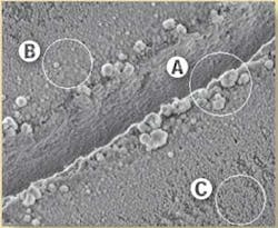
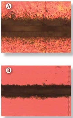
Until now, the main obstacle in applying this technology has been debris formation, which is a result of the condensation of supercooled vapors, partially on the sample surface, partially in the gas phase, via collision with ambient gaseous molecules. The majority of the vapor initially ejected eventually finds itself back on the perimeter of the ablation pattern surface and inside the groove (see Figure 1). Their travel velocity is on the order of several kilometers per second.1
The debris formation deteriorates the feature quality and functionality of the components. It also reduces ablation efficiency because debris from the previous scan can block the laser-beam path for the next scan. Recent investigations have demonstrated the advantage of pico- and femtosecond lasers for the fabrication of fine features with high cleanliness due to the ultrashort-pulse duration. However, the machining speed is still far from industrial expectations.
Methods of reducing debris
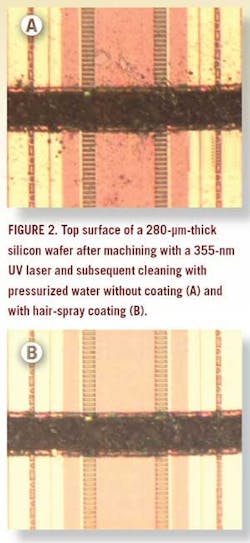
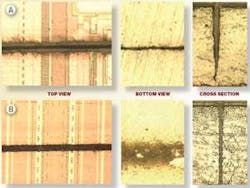
Water-soluble coating in wafer dicing-Various advanced techniques have been tested to minimize the amount of generated debris in wafer dicing. Water-soluble coatings can be deposited onto the workpiece surface to trap debris particles. One of the most common industrial coatings is polyvinyl alcohol (pva). Hairspray or other soap-based solutions can also be used in R&D situations.2 The coating is then washed away using standard pressurized water cleaning techniques (see Figure 2).
“Sandwich” drilling-A so-called sandwich drilling method can eliminate burrs and debris formation in laser drilling. A thin cover plate is applied on the sample surface facing the laser beam. This cover plate collects vapor and molten deposits during the drilling process and also acts as a mask to intercept a portion of the rim of the focused beam. It is insufficient to evaporate the material; the lower part of the radial intensity distribution can only melt or heat up the material and thus affects the hole finishing quality. The back plate covers the other side of the part and is used to avoid deposition of debris and dross on the hole exit.
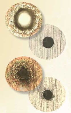
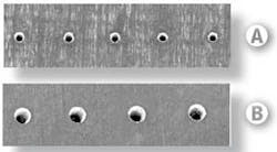
Figures 3 and 4 illustrate holes obtained by percussion “sandwich” drilling with a Q-switched 355-nm UV laser at high pulse energy (100 mJ). The holes drilled on both stainless steel and nickel material are superclean. In contrast, the top of the cover plate shows a crater with a large amount of recast, burrs, and debris. Debris can also be seen at the bottom of the back cover plate.
Laser cutting with defined intensity profile at focus-In many cutting applications, a so called top-hat intensity distribution is preferable. A quasi top-hat distribution simply can be obtained by blocking of the outer region of the focused beam, at a position not far from its focus. Figure 5 depicts the surface of a multiple-pass cutting result of a 280-µm-thick silicon wafer using a lamp-pumped pulsed 532-nm green laser. The “melting” side effect and ultimately the burrs and debris formation could be significantly reduced.
Micromachining with a thin and fast flowing-water film-We have observed better surface cleanliness by applying a steam jet or a confined liquid film. The primary issue is the noncontinuous mode of operation, the optical breakdown of the water film, and the sprinkling of mist or the ejection of the liquid over a large area, which contaminates focusing optics.
Based on that experience, a small syringe-type nozzle was used to generate a hair-thin and laminar flowing liquid film covering the entire laser irradiated area. As the film is thin and flows at high flow rates (greater than 1 m/s), the problem of plasma and bubble generation in the liquid film is avoided, and ablated materials, also inside the kerf, can be carried away efficiently. The nozzle can be fixed to the laser head, and this technique can be applied for different laser wavelengths from 355 to 1064 nm. Significant improvements could be observed in every experiment. For example, we could through-cut a 280-µm-thick silicon wafer with the same number of passes needed in dry cutting, but with a very high level of cleanliness (see Figure 6). Similar results were also obtained in cutting and engraving of copper and aluminum.
Laser-induced transparency and explosive boiling in dicing of silicon wafers-Liquid silicon can be heated above its normal boiling temperature and becomes superheated and transparent to certain laser radiation. The existence of this metastable silicon is due to the lack of a nucleation site at the solid-liquid interface in laser micromachining with nanosecond pulses.4 The transition of superheated silicon from liquid metal to transparent liquid dielectric is due to a strong reduction of electron density in the liquid metal, and the drastic decrease of reflectivity of the transparent liquid silicon is the result of a sudden decrease in dielectric constants.5
By controlling the pulse parameters of a 355-nm Q-switched solid-state laser, we have observed this induced transparency phenomena. We could completely penetrate a 280-µm-thick silicon wafer with a single scan. Normally, multiple scans are required to cut through this wafer and the process results in massive deposition of debris on the top surface. The mechanism of material removal must be based on the generation of vapor bubbles in the superheated liquid silicon as the material ejection does not occur on the irradiated surface, but on the bottom of the silicon wafer (beam exit; see Figure 7). This so-called phase explosion will enable a high throughput and high surface cleanliness wafer dicing.
Different techniques described here are relatively simple to use. To obtain a high-quality micromachining result, laser users should not focus only on choosing the appropriate laser or the correct laser parameters. The use of the presented techniques also should be considered in dealing with debris, recast, burrs, and thermal damage.
Tuan A. Mai is head of KJ Laser Micromachining (a division of KJ Marketing Services), Toronto, ON, Canada; [email protected].
References
- E. Ohmura, I. Fukumoto, and I. Miyamoto, “Scattering of evaporation particles in ultrashort-pulse laser ablation,” Second International Symposium on Laser Precision Microfabrication, Proc. SPIE 4426, p. 66.
- T. Lizotte, “Removal of UV YAG or excimer laser debris after microvia drilling,” Advanced Packaging (January 2002).
- J. Sun and J. P. Longtin, “Ultrafast Laser Micromachining with a Liquid Film,” Proc. ICALEO (2001).
- J. H. Yoo et al., “Evidence of Phase-Explosion and Generation of Large Particles during High Power Nanosecond Laser Ablation of Silicon,” Appl. Phys. Lett.76, p. 783 (2000).
- J. H. Yoo et al., “Explosive Change in Crate Properties during High Power Nanosecond Laser Ablation of Silicon,” J. Appl. Phys. 88, p. 1638 (2000).
null
