NITIN SHANKAR
Editor's Note: Nitin Shankar ([email protected]), a freelance technical journalist, shared with Industrial Laser Solutions his view of selected European industrial laser equipment suppliers exhibiting at LASER World of Photonics 2015, held June 22–25 in Munich, Germany.
The 22nd LASER World of Photonics exhibition, held June 22–25, 2015, in Munich, was the largest show in the world for photonics, a technology connected with functions such as the generation, transmission, amplification, and sensing of light. This article briefly describes selected technologies that could signal trends in micromachining applications.
Photonics-based automated systems
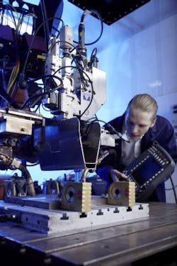
Three Swiss companies, BS-Optics, CP-Automation, and ViDi Systems, partnered to exhibit an automated laser welding system with built-in quality inspection (FIGURE 1).
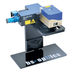
BS-Optics SA specializes in laser systems for welding small parts such as watch bracelets and spiral springs. Its Alice system laser beam (FIGURE 2) can be positioned to an accuracy of ± 1µm, with the vision system ensuring welding position accuracy within 5µm.
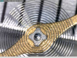
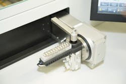
CP Automation specializes in the design and manufacture of automated equipment as needed for volume production, such as welding a spiral spring to a collet (FIGURE 3) or watch bracelet links (FIGURE 4) with cycle times of one part per second.
Finally, ViDi Systems specializes in image analysis software. Inspecting welded seams poses a special challenge and a set of powerful machine-learning algorithms were developed for identifying defective welds.
The above exhibits at the show were good examples of the multidisciplinary approach needed in providing automated welding solutions for the watch industry.
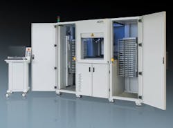
ACSYS Lasertechnik GmbH specializes in laser systems for marking, sawing, and 3D engraving applications, and now offers automated systems for laser engraving operations.
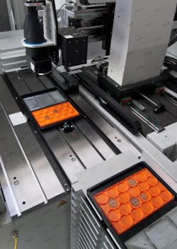
Its Piranha Mutlishift laser engraving machine (FIGURE 5) has a loading station and an unloading station, each station having a capacity of 20 trays. The system moves one tray at a time under a camera (FIGURE 6) and optical parts recognition software identifies the part. The corresponding part program for engraving the part can then be despatched from a central computer.
This is a good example of an automated photonics application for flexible manufacturing.
Minimal-waste dicing and forming
Lasers are being used in innovative technologies to cut parts or make parts without much loss of material.
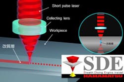
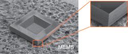
DISCO HI-TECH EUROPE GmbH, a maker of laser saws, offers “stealth dicing” (FIGURE 7)—a method of reducing cutting waste when dicing micro-electromechanical systems (MEMS) components such as micro-sensors from wafers.
In stealth dicing, a short pulsed laser forms a modified layer in a wafer with a tape expander being used to separate the MEMS component (FIGURE 8).
Stealth dicing increases the number of components that can be obtained from a wafer because it is possible to make the necessary street width (cut width) narrower.
It is a dry process and suitable to for dicing MEMS that are vulnerable to pressure from liquids.
Additive manufacturing is another process where parts can be formed with no material loss.
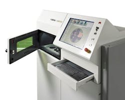
SISMA S.p.A. displayed its Mysint 100 machine (FIGURE 9), a special-purpose 3D printer that uses laser metal fusion to create parts from metal powders and a CAD file.
Ultra-fine layers of powder are progressively laid and melted selectively by a laser source until a metal prototype is formed. The powders used are silver, gold, chrome, or cobalt, and such a process can be of interest to the watch industry for making cases from precious metal alloys.
This form of additive manufacturing will not replace conventional production processes. Although additive-manufactured parts have characteristics superior to those of investment castings, precision parts such as watch cases will need further machining operations.
Ultrafast lasers
Ultrafast lasers emit pulse lengths in the picosecond (10-12) to femtosecond (10-15) range. Such pulses are shorter than the time needed for most energy diffusion processes within the atomic lattice. This technology does away with heat spreading to surrounding areas and the process is referred to as "cold." Nevertheless, heat accumulation can take place with higher repetition rates or higher power.
TRUMPF GmbH + Co. KG and ROFIN-BAASEL Lasertech GmbH & Co. KG are the two German market leaders offering ultrafast laser sources and laser systems.
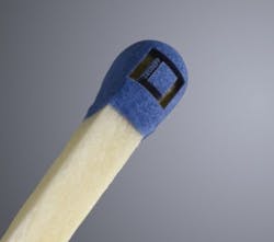
TRUMPF’s TruMicro 5000 laser, available with infrared, green, or UV laser sources, emits ultrafast pulses with durations ranging from 1 to 10ps. The company's leaflet shows a match head with a laser-machined rectangular groove as proof that the process is a "cool" one (FIGURE 10).
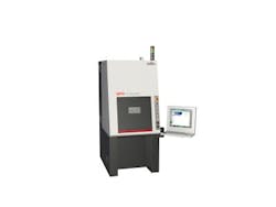
ROFIN's newly developed StarFemto and StarPico ultrafast lasers are designed for cutting brittle materials such as glass or sapphire, as well as high-precision drilling of bores on a micron scale. The company's MPS Compact system (FIGURE 11) can be supplied with a 50W StarPico laser, which generates 15ps pulses to cut and drill surfaces without thermal damage.
The downside is that ultrafast lasers have relatively low cutting speeds. Although they rely on axis speeds of more than 1m/s with low ablation depths per pass, the maximum thickness that can be cut economically is 50 to 100µm.
Waterjet-guided laser
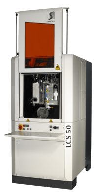
Synova SA offers a slightly faster solution with its LCS 50 system launched at the show (FIGURE 12).
The LCS 50 is equipped with Synova's proprietary Laser MicroJet (LMJ), a waterjet-guided laser cutting technology that allows machining with nearly no heat damage. In this system, the laser is entirely guided within the water jet—similar in principle to an optical fiber.
While conventional lasers have a limited working range of just a few millimeters (ultrafast lasers a few tenths of microns) due to beam divergence, the waterjet-guided laser with a parallel beam can operate over a distance up to 10cm.
With a 5-axis CNC controller and built-in vision system, the LCS 50 is suited for micromachining miniature watch parts and tool inserts.
The lesson learned from the LASER World of Photonics exhibition was that there is no universal laser source that can serve all micromachining applications. While ultrafast lasers seem to work well for 2D applications (layer removal or shallow structures), LMJ technology allows the same quality as ultrafast lasers without depth limitations and is ideal for 3D applications. Users now have the choice to select the laser process best suited for their micromachining applications.
