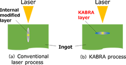
Disco Corporation (Tokyo, Japan) has developed a unique laser wafer slicing method called key amorphous-black repetitive absorption (KABRA; which is trademark-registered and patent-pending, with 40 related patents) that achieves high-speed production of silicon carbide (SiC) wafers, which are anticipated as the next-generation power device material. The process increases the number of wafers produced from a single ingot, and dramatically improves productivity.
The existing methods for slicing wafers from a SiC ingot typically use a diamond wire saw. However, these methods require a number of diamond wire saws for mass-producing wafers because the processing time is long, as SiCs have high rigidity. The number of wafers produced from a single ingot is also small because of the great amount of material lost in the slicing sections. This has been a major factor that increases the cost of producing SiC power devices, hindering their introduction into the market and the widespread use of the SiC power devices.
The unique method forms a flat light-absorbing separation layer (KABRA layer) at a specified depth by irradiating a continuous, vertical laser from the upper surface of the SiC and creating wafers using a previously non-existing slicing method. Conventional laser processing is not suitable for slicing because the modified layer formed by laser irradiation, in principle, extends in the direction of the laser incident (portrait orientation). However, Disco has developed this laser slicing method focusing on two facts: 1. that SiC can be decomposed by a focused laser and separated into silicon (Si) and carbon (C) in an amorphous state, and 2. that the light absorption coefficient is approximately 100,000 times larger than that of SiC. As a result of this development, the company has succeeded in forming KABRA layers inside the ingot both vertically and in the direction of the laser incident, finding the optimal laser slicing method. In addition, this process can be applied to various types of SiC ingots, including single-crystal (4H, 6H, and semi-insulation) and multi-crystal ingots.
One of the major characteristics is that this process can be applied to monocrystal ingots, regardless of the off-angle of the crystal c-axis.
KABRA forms a layer that becomes the base point for separating the wafer by decomposing SiC into amorphous silicon and amorphous carbon with continuous laser irradiation, and then making the black amorphous efficiently absorb the light. Its advantages include greatly reduced processing time, no need for the lapping process, and the number of wafers produced increases 1.5 times more than that of existing processes.
For more information, please visit www.disco.co.jp.

David Belforte | Contributing Editor
David Belforte (1932-2023) was an internationally recognized authority on industrial laser materials processing and had been actively involved in this technology for more than 50 years. His consulting business, Belforte Associates, served clients interested in advanced manufacturing applications. David held degrees in Chemistry and Production Technology from Northeastern University (Boston, MA). As a researcher, he conducted basic studies in material synthesis for high-temperature applications and held increasingly important positions with companies involved with high-technology materials processing. He co-founded a company that introduced several firsts in advanced welding technology and equipment. David's career in lasers started with the commercialization of the first industrial solid-state laser and a compact CO2 laser for sheet-metal cutting. For several years, he led the development of very high power CO2 lasers for welding and surface treating applications. In addition to consulting, David was the Founder and Editor-in-Chief of Industrial Laser Solutions magazine (1986-2022) and contributed to other laser publications, including Laser Focus World. He retired from Laser Focus World in late June 2022.


