Micromachining with laser-tailored pulses
New fiber laser architecture
By Mathew Rekow and Richard Murison
Novel laser micromachining processes are finding their way into more and more industrial applications. New wavelengths, shorter pulse durations, decreasing cost, and increasing reliability are just a few of the parameters driving this growth. Traditionally, finding the optimal laser process for these new applications has been problematic and has often required the development of new lasers to achieve the right combination of laser parameters. Furthermore, little attention has been given to the subtleties of the temporal distribution of energy within a single laser pulse. A new master oscillator power amplifier (MOPA) fiber laser architecture has emerged that overcomes these limitations and has resulted in a single laser platform that can address a huge range of applications. This article showcases three micromachining applications that have been improved or enabled by this new laser technology and demonstrates the advantages of tailoring the temporal energy distribution of each laser pulse to fit the application requirement.
The tailored-pulse laser
The PyroFlex-25, a 25 W, 1064 nm pulse programmable fiber laser, is applied to the three applications detailed in this article [1]. Unlike more traditional lasers, this fiber laser technology allows pulse durations to be varied from approximately 2 to several 100s of nanoseconds, independent of laser repetition rates, which can be varied up to 500 kHz. In addition, each pulse can be arbitrarily programmed to generate a specific desired temporal profile of instantaneous laser power. Pulse trains comprised of these shaped pulses can be applied to the micromachining process at high repetition rates.
CIGS solar cell scribing
CIGS (CuInGaSe2) has become a popular material for the production of thin film PV panels. CIGS now holds the world record of 20.1% [2] efficiency for thin film single junction cell efficiency. With any new material comes new challenges, and CIGS has been no exception. While laser scribing has long been the process of choice to form a-Silicon and CdTe monolithic interconnects, typically referred to as the P1, P2 and P3 scribe processes [3], CIGS has until now defied laser processing for the P2 and P3 steps. Thermal effects, giving rise to an increase in electrical conductivity of the film in the laser processed areas, are detrimental to the solar cell electrical performance. Even picosecond laser process results are not completely free of this detrimental heat effect as evidenced by the melted edges and residue (see FIGURE 1a).
Utilizing the pulse tailoring capabilities of the programmable fiber laser, we have shown that a narrow process window exists in the low nanosecond regime within which a CIGS film can be scribed with virtually no heat effect [4]. FIGURE 1b and FIGURE 1c contrast the result obtained in scribing a CIGS P2 film when all laser pulse energy is confined within a 5 ns process window with the case where a fraction of the energy is allowed to extend in time outside the process window. The latter case may correspond to the case of a Q-switched pulse with a relatively long temporal tail. These contrasting laser pulse shapes are illustrated by the animation in FIGURE 2. Both pulses have equivalent energy and FWHM, but the temporal distribution of energy is markedly different.
CdTe solar cell scribing
CdTe is the most widely established material system for thin film PV modules. Laser scribing has been used with great success for the CdTe P1, P2, and P3 scribing steps and a standard process sequence is well established in the industry. In particular, the common methodology that has been adopted for the P1 step results in exposure of the soda lime glass (SLG) substrate. In turn, Na diffusion from the glass into the CdTe is detrimental to the performance of the CdTe film [5]. To mitigate this problem, commercial processes implement the P1 scribe after the CdTe deposition and the resulting groove is then backfilled with a photo-resist to serve as both a Na diffusion barrier and to serve as mechanical support for the overlying conductive layers and to prevent subsequent electrical shunting. This photo-resist application process accounts for a significant fraction of the cost for the capital equipment in a CdTe module production line.
This model then implies that careful temporal control of the energy input should permit precise control of the depth of the ablation pit. Applying these findings, the pulse tailoring feature of the laser was used to create a pulse that starts with an initially high peak power for 2 ns to start the reaction. The pulse peak power was then empirically adjusted after the initial 2 ns to the minimum required to keep the reaction proceeding and pit depth growing, thus creating the "chair" shaped laser pulse of FIGURE 4.
It was found that the peak power could be reduced by more than 95%, and the reaction would continue to completion. Furthermore, we discovered that by controlling the duration of the tail, the pit depth could be precisely controlled to an accuracy of 10’s of nm (FIGURE 4). FIGURE 5 shows the ideal pulse and the video clip illustrates how it was changed to perform this experiment.
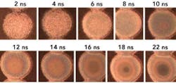
FIGURE 6 shows how the pit morphology evolves as the duration of the pulse tail is increased. Work on this project is ongoing.
Silicon dicing and grooving
Silicon grooving and cutting is of interest to both manufacturers in the solar cell and microelectronics industries. Silicon solar cells require a cut along the periphery of the cell as a final step to electrically isolate the emitter from the back contact, which is typically done with a laser. In the microelectronics industry, as wafers grow ever thinner, laser-based dicing is displacing the diamond saw as the preferred chip singulation method. Due to relatively high heat effect and beam penetration depth of 1064 nm light, Q-switched UV lasers are becoming the laser of choice for singulation applications, whereas cost and throughput have favored high power 1064 nm or CO2 lasers for edge isolation.
In silicon, the absorption at 1064 nm is known to be relatively low at room temperature. When a 1064 nm laser pulse interacts with the silicon bulk, much of the energy penetrates deeply and is lost to thermal conduction [8] and results in a deeper melt zone formation. This has the dual effect of making the process less efficient and increasing the amount of remaining debris. It has been found that introduction of a very low power “pre-pulse” has the effect of locally increasing the temperature and therefore absorption. Thus utilizing the pulse tailoring feature of the fiber laser, it is possible to increase the absorption coefficient of the material in advance of the primary laser pulse.
To test this premise, the laser system was configured to cut 20 µm wide grooves in a multi-pass configuration at 800 mm/s. Single 2 ns, 100 µJ, pulse trains at 100 kHz determined the average dicing speed in a multi-pass configuration for a 50 µm thick silicon wafer. A 5 µJ pre-pulse, 8 ns in duration was added, and we varied the delay between the pre-pulse and the primary machining pulse. This experimental laser pulse configuration is depicted in FIGURE 7 and the video demonstrates how the pulse delay was varied..
The results of the experiment showed that there was a marked increase in cutting speed of about 1.7X when only 5% more energy was added in the form of a pre-pulse with a delay of about 20 ns. FIGURE 8 shows that the 20 ns delay between the pre-pulse and the primary pulse represents an optimum value. The morphology of the cut also showed a decrease in the quantity of debris and size of the recast berm with the introduction of the pre-pulse.
FIGURE 8. Effect of the pre-pulse delay on the effective cutting speed for a silicon wafer.
Conclusion
The three test applications clearly illustrated the benefit of controlling the temporal shape of a laser pulse. In the first test, a previously unknown and narrow process window for CIGS P2 and P3 scribing was found by limiting the extent of the laser pulse in time to 5 ns, and producing a pulse with a “rectangular” temporal profile. In the second test, TCO material was precisely removed from a glass substrate by controlling the temporal energy input. The depth of the groove was controlled to an accuracy of 10s of nm by varying the duration of the pulse tail ns by ns.
Finally, in the last test, the removal rate of silicon in silicon cutting was enhanced by adding a very low energy pre-pulse to increase the absorption coefficient for the primary machining pulse. These three test applications confirm that control of the temporal shape of a laser pulse influences the resulting laser process in profound ways. In some cases, new processes are enabled and, in others, processes are markedly improved. In all cases, the pulse tailoring enabled a deeper and more thorough understanding of the laser material interaction process.
References
1. R. Murison, et al., US Patent 7742511, 2008.
2. Claudia Brusdeylins, Press Releases, Zentrum für Sonnenenergieund und Wasserstoff-Forschung Baden-Württemberg (ZSW). [Online] April 28th , 2010. [Cited: July 21, 2010.] http://www.zsw-bw.de/fileadmin/ZSW_files/Infoportal/Presseinformationen/docs/pi05-2010-ZSW-Worldrecord-TF-CIGS.pdf.
3. A. R. Jha, "Solar cell technology and applications," Auerbach Publications, Boca Raton, 2009. p. 21.
4. M. Rekow, R. Murison, C. Dunsky, et al., "CIGS P1, P2, P3 scribing processes using a pulse programmable industrial fiber laser," 2010.
5. N. Romeo, A. Bosio, R. Tedeschi, V. Canevari, "Growth of polycrystalline CdS and CdTe thin layers for high efficiency thin film solar cells," Materials Chemistry and Physics, 2000, Vol. 66, Issues 2-3.
6. K. Von Rottkay, M. Rubin "Optical indices of pyrolytic tin-oxide glass," Berkely, LBNL, 1996, 38586.
7. L. V. Gurvich, I. V. Veyts, C. B. Alcock, "Thermodynamic properties of individual substances: Part 1, Volume 2, Elements C, Si, Ge, Sn, Pb and their compounds," Hemisphere Publishing Corp., Moscow, 1979. ISBN 0-89116-533-9.
8. Sami T. Hendow, Sami A. Shakir, "Structuring materials with nanosecond laser," 10, s.l., Optical Society of America, 2010, Vol. 18.
Mathew Rekow ([email protected]), is a principal applications engineer at PyroPhotonics Lasers, Fremont, Calif., a subsidiary of ESI Inc. Richard Murison is chief technology officer and director of product marketing at PyroPhotonics Lasers, a subsidiary of ESI Inc.


