Nanoimprint lithography process for high-volume manufacturing

Oct. 22, 2014
EV Group (EVG) has introduced its SmartNIL large-area nanoimprint lithography (NIL) process.

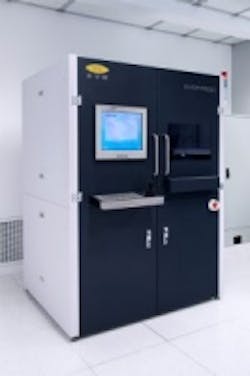
St. Florian, Austria - EV Group (EVG) has introduced its SmartNIL large-area nanoimprint lithography (NIL) process. Available on all of the company's NIL platforms, the process provides a low-cost, large-area, and high-volume-manufacturing solution for a variety of advanced devices, including photonic-based devices such as LEDs, lasers, and photovoltaics; microarrays and nano-devices for medical devices and bioengineered applications; and advanced storage media, including newly emerging forms of non-volatile memory (NVM).

Features include a large full-field imprint area (up to 200mm), processing of >40 substrates/hr for 200mm substrates, and integrated soft stamp fabrication technology to reduce tool footprint and provide replication in less than 10 min. Self-cleaning properties reduce particle contamination and improve overall processing yields, while a room-temperature process avoids thermal mismatch and long-range structure distortion for improved alignment accuracy. Patterning on highly topographical structures is also possible.

For more information, please visit www.evgroup.com.
Sponsored Recommendations

Hexapod 6-DOF Active Optical Alignment Micro-Robots - Enablers for Advanced Camera Manufacturing

Dec. 18, 2024
Optics and camera manufacturing benefits from the flexibility of 6-Axis hexapod active optical alignment robots and advanced motion control software

Laser Assisted Wafer Slicing with 3DOF Motion Stages

Dec. 18, 2024
Granite-based high-performance 3-DOF air bearing nanopositioning stages provide ultra-high accuracy and reliability in semiconductor & laser processing applications.

Free Space Optical Communication

Dec. 18, 2024
Fast Steering Mirrors (FSM) provide fine steering precision to support the Future of Laser Based Communication with LEO Satellites

White Paper: Improving Photonic Alignment

Dec. 18, 2024
Discover how PI's FMPA Photonic Alignment Technology revolutionized the photonics industry, enabling faster and more economical testing at the wafer level. By reducing alignment...

Voice your opinion!

To join the conversation, and become an exclusive member of Laser Focus World, create an account today!