Forgery-proof laser-holographical product identification
Chemnitz, Germany -- Clear, complete identifiability of products is becoming more and more important for manufacturers in various branches of industry, for comprehensive traceability of products. Originality has to be guaranteed especially for expensive and security-related components. Piracy of products poses a serious problem worldwide—the economic damage caused by product piracy amounts to about €30 billion every year in Germany, for example—generating significant losses in sales and often causing irreparable image loss to the affected companies.
A very high security standard for components is needed especially in aerospace engineering, vehicle manufacturing, and the medical industry, as the usage of forged products could have fatal consequences in these branches.
Currently, components are marked by conventional laser systems or by needle stamping. However, the markings of both techniques can be easily copied by the use of suitable equipment.
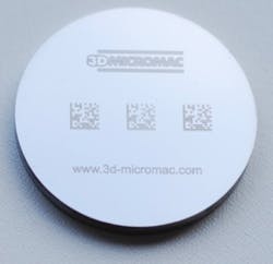
The laser marking technology developed in the ZIM-project "perfekt" offers a new possibility to mark high-end products with metal or silicon surfaces entirely unforgeable. Members of the project consortium include 3D-Micromac AG, Laser-Laboratorium Göttingen e.V., the University of Applied Sciences Bielefeld, Kappa opto-electronics GmbH, SURA Instruments GmbH, and OLPE Jena GmbH.
In contrast to conventional laser markings, the depths generated with this new technology amount to only 100-200 nm, so the basic material is not influenced by the laser. The laser-holographical marking also resists forgers' "reverse engineering" efforts, since it is not possible to determine the kind of DOEs used or their position to each other by reading the pattern.
Laser-holographical product identification offers a lasting solution to produce unique and forgery-proof labelings and equips the companies with a means to resist the rapidly growing amount of pirated products. The technology is originally being targeted to metal or silicon surfaces; "in the near future" it will be possible to add safety features to glass and ceramics, 3D-Micromac claims.

