By Colin Moorhouse, Coherent Inc.
The demand to reduce the size, weight, and material cost of leading-edge devices has resulted in a requirement for precision micromachining to improve product development in several industries. Examples include making smaller and more powerful smartphones with brighter displays, reducing the cost and increasing the efficiency of solar cells, and machining the latest bio-absorbable medical stents. The unrelenting pace of innovation in high-tech industries has led to ultrafast (picosecond) industrial lasers becoming important tools for applications requiring high precision. These lasers' unique operating regime (megawatts of peak power) enables clean cutting and patterning of sensitive materials and thin films used in a number of novel devices as well as micromachining of wide bandgap, "difficult" materials such as glass. In several instances, the picosecond laser is replacing multi-step photolithography with a single-step direct-write laser process; in other cases it supplants traditional cutting/drilling processes because it eliminates costly post-processing cleaning steps, such as stent manufacturing. With a choice of near-IR, green, or ultraviolet output, these lasers can micromachine almost any material bringing new technologies to market successfully.
Patterning OLEDs
Organic, flexible electronic devices have many intrinsic advantages including their light weight, thin dimensions, and transparency. In particular, flexible organic light-emitting diodes (OLEDs) have tremendous potential for displays, since they consume less power than other displays that use backlighting, as well as for general lighting. An OLED is formed by an organic emissive layer, light emitting polymer (LEP), sandwiched between an anode and a cathode layer.
FIGURE 1. Schematic of a basic OLED structure.
OLEDs can be manufactured on reel-to-reel production lines, using screen/inkjet printing for patterned deposition of device circuitry 1, 2. However, these technologies are limited in terms of the minimum achievable feature size, and the ability to maintain thickness uniformity within each layer. Large-area uniformity has been demonstrated using full-area deposition techniques such as spin coating, and laser patterning of these layers is extremely attractive for roll-to-roll processing.
Ultraviolet (355 nm) nanosecond lasers, which have proven themselves in numerous other electronics micromachining applications, have two limitations for this type of patterning. First, they produce some molten material or debris, which cannot be tolerated due to the approximately 100 nm thickness of the layers. Second, it is extremely difficult to prevent damage to the underlying layers due to the thermal penetration depth of the nanosecond laser pulse being greater than the thickness of the layers.3 In contrast, picosecond lasers can readily deliver debris-free patterning and selective depth control, because material removal occurs before the material can respond to the acoustic/thermal stress.4 However, to achieve selective removal of thin films, it is critical to maintain the laser fluence close to the laser ablation threshold, Fth. This quantity can be estimated by making a curve fit to a plot of the single-shot laser-ablated crater diameter against the pulse energy.5
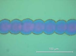
As an example, a LEP layer has been laser scribed from a SiO2 barrier (this material was provided by the Holst Centre as part of the fast2light project6), where a fluence of 1.6*Fth is required to give the desired quality shown in FIGURE 2. The superior pulse-to-pulse stability (<2%) of Coherent's fiber-based Talisker laser is particularly advantageous for fine control of the pulse energy to make consistent scribes, and there is no melt or debris on the surface without any post-laser cleaning. The high laser repetition rate of 200 kHz allows a fast scribing speed of 6 m/s, scalable to 15 m/s using the ultraviolet 500 kHz Talisker 500.
Silicon solar cells
Solar cell manufacturers are currently striving to reach cost parity with grid power. There are two ways to move toward this goal: reduce cell cost, and improve the cell light-conversion efficiency. The majority of solar cells are currently based on silicon wafers, and the use of thinner <e;200 μm wafers is helping reduce material costs. One way to increase the efficiency of these crystalline silicon (c-Si) solar cells is to use a backside passivation layer to reduce recombination losses. To make electrical contacts to the cell, through-holes must be drilled through the passivation layer, typically formed from silicon dioxide/silicon nitride -- this must be accomplished with minimal damage to the underlying crystalline silicon to maintain the cell performance and ensure good ohmic contact for current collection. Picosecond lasers offer a lower-cost, direct-write alternative to photolithography for this task, eliminating the cost of vast quantities of chemicals. Specifically, studies have found that 355 nm picosecond pulses offer selective removal of the dielectric layers with little or no damage to the underlying silicon.7 Furthermore, comparisons demonstrate that the ablation threshold fluence for UV picosecond lasers is lower than that of IR femtosecond lasers.8 These results have been verified in FIGURE 3 with a laser ablation threshold, Fth value of 0.02 J/cm2 observed for 355 nm, 10 ps pulses, compared to 0.08 J/cm2 for 1030 nm, 500 fs pulses. The lower threshold value enables patterning at lower energy and hence reduced damage to the underlying silicon.
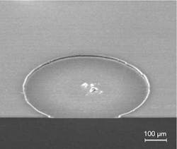
FIGURE 4 shows the exposed silicon surface following selective removal of a 100 nm SiO2 passivation layer from silicon using 355 nm picosecond pulses, at an optimal fluence of ~1.5*Fth. Importantly, there are no melt features in the silicon as can be found with nanosecond laser processing, thus eliminating the requirement for post-laser chemical etch treatments. In addition, no sub-surface damage is visible -- some small particles in the center remain from the picosecond laser ablated dielectric layer, but these can be removed easily by air. The high pulse repetition rate of the Talisker laser allows contact holes to be drilled at rates of 200,000/second or more. Inclusion of this process within c-Si solar fabrication allows efficiency gains of ~0.5-0.7%, which represents a significant advantage for solar cell manufacturers.
Thin-film solar cells
Despite improvements in various c-Si architectures, many in the solar industry believe that thin-film solar designs are the long-term future, and represent the approach that is most likely to achieve grid parity. This is because of the smaller amount of semiconductor material needed in these designs, plus the potential for low-cost mass production via reel-to-reel processing of flex substrates. Materials such as CuInSe2 (CIS) and CuInGaS2 (CIGS) exhibit wide optical absorption across the visible spectrum, making them attractive as efficient photovoltaic materials in these devices. A typical thin-film solar cell structure is shown in FIGURE 5, where the high light absorption means that the active layer is only ~1 μm thick, greatly reducing material costs compared to c-Si solar cells.
FIGURE 5. Schematic of a typical CIGS structure and P1, P2, P3 scribes.
To make a solar cell from this structure, P1, P2 and P3 scribes are required as indicated in FIGURE 5 (and havebeendescribednumeroustimes in ILS magazine). P1 scribes serve to isolate the back contacts of adjacent cells by patterning the back-contact metal, which is usually molybdenum (Mo). P2 scribes open contacts from the frontside to the backside of adjacent cells in order to connect the cells in series maximizing the voltage output. P3 scribes are required to isolate the front contacts of the cells by cutting through the transparent conductive oxide (TCO) layer and CIGS down to the Mo back contact. P3 scribes are currently made mechanically with mechanical "pins," but these scribes are prone to leaving residual material and can cause chipping of the layers, and the mechanical pins also require frequent recalibration/maintenance. In addition, when the supporting substrate is metal or plastic, mechanical scribing can damage these layers, making a laser process more attractive.
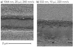
One of the main difficulties with laser ablation of CIGS has been that on melting, it undergoes a phase transition from semiconductor to metal. Hence, any molten CIGS in the scribe may potentially short-circuit the cell, reducing efficiency. However, using a picosecond laser, together with careful control of the laser fluence, it is now possible to produce high-quality clean scribes as shown in FIGURE 6(a) using 1064 nm pulses. An improved, extremely smooth, mirror-like Mo surface is obtained using 532 nm pulses as in FIGURE 3.(b). This is most likely due to the reduced plasma generated and shorter optical penetration depth at 532 nm. In both cases, complete removal of the CIGS from the scribe has been demonstrated, with no molten material or electrical contact between the TCO edges and molybdenum back-contact layer, resulting in high efficiency solar cells.
Laser drilling of transparent materials
The strength, chemical inertness, and high transparency of glass are the reasons for its wide use in many consumer electronics, such as touch screens, handheld devices (tablets, smart phones, etc.), and flat-panel TVs. Also, future devices are anticipated to rely more heavily on glass to provide structural rigidity and to create features holes need to be drilled through the glass. However, a glass substrates get thinner to support smaller and lighter devices, traditional glass-drilling techniques struggle to maintain the quality demanded -- even established industrial lasers such as carbon dioxide (CO2) and nanosecond lasers have difficulty drilling these holes without significant microcracking and chipping. It is critical that edge cracking and residual edge stress are avoided in touchscreens where the panels almost always break from the edge, even when stress is applied to the center.
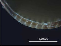
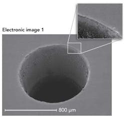
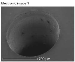
The high peak power of picosecond lasers can avoid this problem, and since glass is essentially transparent to visible wavelengths, 1064 nm offers the highest average processing power for maximum removal rates whereas the UV wavelength is better suited for thinner glass panels. As examples, FIGURES 8 AND 9 show high-quality 1 mm-diameter holes drilled in 1 mm-thick D236T glass and quartz using 1064 nm picosecond pulses. The microchips on the edges are typically only a few microns -- and more crucially, there are no microcracks on the edges or sidewalls, which prevents fractures, making this process ideal for handheld devices.
Summary
Picosecond lasers are now industrially proven, robust tools, offering sturdy and reliable performance suitable for a wide variety of industrial applications, such as the examples described here. The combination of short picosecond pulses, excellent pulse-to-pulse stability, and high repetition rates deliver precision cuts and patterns with sharp, clean edges with no requirement for post-process cleaning. Additionally, their fine control of laser energy and pulse-to-pulse stability enables blind holes, cuts, and scribes to be created with unprecedented accuracy, even in delicate materials such as polymers. Moreover, the wavelength flexibility (1064 nm, 532 nm and 355 nm) and excellent beam quality (M2<1.3) of the Talisker Ultra picosecond laser platform can be utilized for laser processes requiring extremely tightly focused laser beams with high peak power.10,11,12 The Talisker 500 shares a similar platform design with a single-output wavelength for optimal performance in production environments which is particularly advantageous for precise, small feature sizes in glass, which is gaining market share in emerging applications as alternatives to existing laser and non-laser processes.
References
[1]. T.R. Hebner et al., "Ink-jet printing of doped polymers for organic light emitting devices,"Applied Physics Letters 72(5), 519-521 (1998).
[2]. G.E. Jabbour et al., "Screen printing for the fabrication of organic light emitting devices,"IEEE Sel.Top. Quantum Electron. 7(5), 769-773 (2001).
[3]. A.F. Lasagni et al., "Direct laser interference patterning of poly(3,4-ethylene dioxythiophene)-poly(styrene sulfonate) (PEDOT-PSS) thin films,"Applied Surface Science, vol. 22, pp. 9186-9192, 2009.
[4]. D.M. Karnakis et al., "Ultrafast Laser Patterning of OLEDs on Flexible Substrate for Solid-state Lighting,"Journal of Laser Micro/Nanoengineering, vol. 4, pp. 218-223, 2009.
[5]. P.T. Mannion et al., "The effect of damage accumulation behaviour on ablation thresholds and damage morphology in ultrafast laser micro-machining of common metals in air,"Applied Surface Science 233(1-4), pp. 275-287, 2004.
[6]. www.fast2light.org
[7]. V. Rana and Z. Zhang, "Selective Removal of Dielectric Layers using Picosecond UV Pulses,"Proceedings of SPIE, vol. 7193, pp. 719321, 2009.
[8]. M. Bähr et al., "Ablation of dielectrics without substrate damage using ultrashort pulse laser systems,"Proceedings 25th EUPVSEC, 2010.
[9]. P. Törmala et al., "Bioabsorbable polymers: materials technology and surgical applications,"Proceedings of the Institution of Mechanical Engineers, Part H: Journal of Engineering in Medicine, vol. 212, pp. 101-111, 1998.
[10]. Coherent white paper: "Flat panel display defect repair using high peak-power picosecond lasers."
[11]. Coherent white paper: "Micromachining of sapphire wafers for LED production using picosecond lasers."
[12]. Coherent white paper: "Micromachining of glass using a fiber-based, high average power picosecond laser."
Colin Moorhouse ([email protected]) is with Coherent Inc., Santa Clara, CA.

