Web Exclusive: Laser soldering compression method for fine-pitch, thin-die applications
A novel soldering methodology has been tested and proven in forming robust, high-yield, and cost-effective electronic interconnects in the semiconductor and surface-mount industries. This was accomplished in an in-line mass manufacturing environment. The application consisted of a 70-µm-thick die with a 40 µm copper pillar and 25 µm tin-silver cap. The printed circuit board (PCB) thickness was 350 ±20 µm for a total system thickness of ±460 µm. The concern with developing a soldering process for this application and similar ones is the proper coalescence of the component and pad terminations. Warpage, dimensional variations, and proper contact in conjunction with soldering parameters are critical in achieving reliable, consistent interconnects within a robust soldering process.
Laserssel (Dover, NH) has developed a method to ensure a repeatable soldering process using its novel area laser solder reflow (LSR) technology in conjunction with compression to enable the end user to effectively produce reliable, high-yield interconnects. In this case study, two methods were developed to characterize the impact of compression on yield. The dimensions for the PCB and die are listed in the table.The soldering process was developed to solder 30 die simultaneously using the area laser. The typical area LSR process consists of 1–10 seconds of exposure time to the defined area. This application requires three distinct areas to be soldered; the total process time is approximately 24 seconds. Then, the separate soldering processes were developed—one used compressive force on the 30 die, while the other soldering process did not.
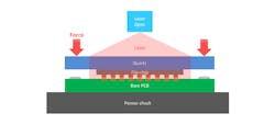
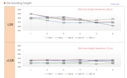
The compressive force was accomplished using a controlled quartz plate incident on the defined soldering area, as illustrated in FIGURE 1.Given the dimensions of the die and PCB, the maximum deviation is <15 µm, inclusive of any die warpage to develop consistent interconnects. The results conclusively show the benefit of compressive force on the system height after soldering. Without compressive force, the maximum height deviation was 28 µm across six die, while with compressive force, the maximum height deviation was 10 µm across six die (FIGURE 2).
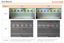
This impact of the 28 µm system height deviation is widespread occurrence of opens due to die warpage, as shown in FIGURE 3.In summary, for specific applications, the use of compression enables the end user to eliminate die warpage, resulting in a robust, repeatable, high-yielding soldering process.
For more information, please visit laserssel.com.


