High-throughput ultrashort-pulse laser micromachining
Ultrashort-pulse (USP) lasers—that is, lasers with pulse durations as short as a picosecond or even less—have created a lot of interest in recent years. They can process almost every material, and they do so with micron precision without splatter or thermal side effects. Their only limitation has been average power and, therefore, throughput. Now, kilowatt sources for picosecond or femtosecond pulses have become available, which raises the question how to turn increased power into higher productivity. In this article, we discuss several ways towards higher throughput for drilling and surface structuring processes.
The laser sources
Now, USP lasers with 150 W average power and 150 µJ pulses are available for purchase from stock, with more-powerful machines offering kilowatt power or millijoule pulses from a growing number of vendors. The German Fraunhofer Gesellschaft has announced multimillion-dollar efforts to develop laser sources and process technology of 10 kW or more within the next 2–5 years.
There are several ways to upscale USP lasers. Typically, the developers increase the energy per pulse and/or the repetition rate of the source. Both numbers, when multiplied, result in the available average power of the source as a simple means to compare laser sources. In the old world of continuous-wave lasers, more power meant more productivity. For USP lasers, things become more difficult since the price of the system is only justified if the precision of the processing is maintained.
It should be mentioned that productivity may also depend on other parameters. For certain materials, better ablation results can be achieved by using shorter pulses or shorter wavelengths. A recent article in Industrial Laser Solutions showed details on upscaling the ablation rate. The underlying effects strongly depend on the kind of material.
But the key question is: How can more power be turned into higher throughput?
Some tweaks and rules
The ablation process of ultrashort pulses is complex and has been subject to extensive research. One simple conclusion is that if USP laser pulses at a high repetition rate illuminate the same spot, then heat is accumulated in the workpiece material and the benefit of “cold” ablation (that is, without heat-affected zone) vanishes. So, just increasing the number of pulses does not lead to higher productivity with the same precision.
In general, the more energy you put into one pulse, the more you ablate, but the plus in ablated volume gets smaller with increasing energy. And soon, the quality of ablated structures suffers. There are some rules of thumb to find an optimum energy for ablation.
At this point, we can see that the physical quantity that has most influence on the structuring result is the fluence—that is, the pulse energy divided by the focal spot size. It has been found that for USP lasers, ablation becomes most efficient when the fluence is equal to e2 (roughly 7) times the threshold fluence.
A major question for surface structuring processes is the use of pulse bursts, where a short sequence of pulses is applied. Only the first pulse ablates a pristine surface, all following pulses may see a plume above the focus that absorbs part of the energy. Thus, the ablation, for example, of five separate pulses with a separation of one second will always be higher than for five pulses in one burst. However, a burst will remove more material per second. A detailed discussion of USP laser burst processing can be found elsewhere.1
20,000 holes drilled per second
One promising path to higher productivity with high-power USP laser sources is a division of the powerful beam. Splitting the beam into a large number of beamlets allows for parallel processing. In particular, with periodic structures, one may use a large number of similar beamlets and realize substantial productivity gains.
The key for this way of upscaling is the proper approach to split a powerful beam into many beamlets with similar properties. A typical solution is diffractive optical elements (DOEs), which are flat optics with a complex inscribed structure that diffracts the optical wave of the beam. This way, it can create one spot, one line, or even more than 100 similar beamlets out of one beam. While it is easy to create a multitude of copies of the original beam, one can also use the DOE to create special beam profiles such as flat-top or Bessel beams.
The surface structure of a DOE is etched into the glass with extreme precision using lithography techniques. As a result, the DOE is a flat piece of glass that creates a static beam distribution. Most often, it requires further lenses and scanning technology for industrial processing.
The experts at the Fraunhofer Institute for Laser Technology (Fraunhofer ILT; Aachen, Germany) have been working on such beam shaping concepts since 2012. In 2019, they reached a record of 20,000 holes/second drilled into a thin metal film. They used a DOE with more than 200 beamlets to drill holes of 1 µm diameter in a 10-µm-thick foil for filter applications.
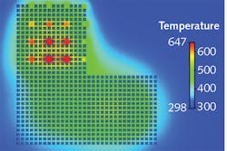
Even with USP lasers, some heat remains in the workpiece, which becomes relevant at high pulse energies and/or high repetition rates. With short spatial distances between holes, it becomes necessary to employ customized thermal management to avoid thermal damage. Therefore, a team at Fraunhofer ILT developed a software for a detailed simulation of the physical processes during and after the laser absorption. With this tool, thermal effects can be studied and processing patterns can be tested (FIGURE 1).
The concept of a simple pattern for drilling or surface patterning can be systematically extended towards more flexibility. Therefore, the experts at Fraunhofer ILT are investigating several different multibeam concepts. In a European project called “MultiFlex,” they are developing a sort of optical dot-matrix printer where a 1 kW USP laser beam is split into a matrix of 60 beams. These beams will be sent through a set of acousto-optical modulators (AOMs) so that they can be switched on and off independently. So far, they have shown the control of 8 beamlets in one AOM. The project targets an 8 × 8 beam matrix. It should be mentioned that the typical switching time of an AOM is less than 1 µs, so a megahertz triggering of the laser matrix printer seams feasible.
The next step towards more flexibility is a complete dynamic beam shaping tool. There, a liquid-crystal modulator replaces the DOE. Such a spatial light modulator (SLM) can create arbitrary patterns for diffraction. The switching time is typically in the order of 10 ms, so a 100 Hz switching of the patterns is realistic.
When comparing these three concepts, we see a number of differences. Beam shaping with a DOE is static, but has high precision and allows for high durability in industrial applications. If we add AOMs to this concept, we can very rapidly turn on and off single beamlets and generate varying beamlet distributions. The SLM allows for a change of the whole pattern, but this is comparably slow and SLMs have a comparatively low damage threshold.
Applications
A first application example has already been mentioned. Drilling 20,000 micron-sized holes into a metal foil gives a good microfilter. With such a metallic surface filter, certain particles can be separated. This works, for example, in water filters for multiresistant microbes or for microplastics as well as in many other biotechnological applications. The use of microfilters is also interesting for the food industry—for example, in the field of sterile filtration, where all kinds of microorganisms have to be retained. Other possible applications include the filtration of fine dust in air (PM classes from 10 to 1) or the mechanical separation of white and red blood cells in medical technology, to name just a few applications for microfilters.
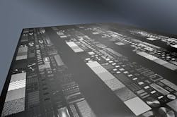
Engraving printing rollers (or more-general cylinders for roll-to-roll processing) is another promising application that has been shown in industrial processes. At the last UKP Workshop, Stefan Brüning (Schepers) reported about a 500 W laser with 10 ps pulses to ablate 200 µm deep structures from a copper surface using individually addressable multibeams (FIGURE 2). He achieved an effective output of 20 W per channel in a 2 × 8 beamlet system. The same technology was applied to hardened steel and aluminum cylinders.Researchers from TRUMPF (Ditzingen, Germany) showed the use of a SLM for flexible beam shaping at the 2019 LASE conference in San Francisco, CA. They created various Bessel beams and demonstrated glass cutting with these beams. Furthermore, they created a number of special beam profiles such as rectangular, T-shape, or a matrix of 15 squares to prove the ability of the system to create sharp edges. The beam profiles were used for processing tests and achieved a resolution better than 1000 ppi. A number of electronic applications such as microvia drilling could benefit from this technology.
Outlook
With the advent of high-power picosecond and femtosecond lasers, new solutions are needed to turn the increased average power of the laser systems into increased productivity. Multibeam optics offer several opportunities to upscale machining processes. Depending on the type of optics, there are static solutions (for example, DOE) for making periodic structures, or slower dynamic solutions (SLM) for processing of changing patterns. Furthermore, with sets of AOMs, it is possible to generate rapidly switchable beam patterns just like with a matrix printer. All of these solutions are now applied in industry-grade machines. Challenges remain for beam optics and scanning technology.
REFERENCES
1. J. Finger et al., Adv. Opt. Technol., 7, 3, 145–155 (2018).
2. D. Flamm et al., Proc. SPIE, 10904, 109041G (Mar. 4, 2019).

Andreas Thoss | Contributing Editor, Germany
Andreas Thoss is the Managing Director of THOSS Media (Berlin) and has many years of experience in photonics-related research, publishing, marketing, and public relations. He worked with John Wiley & Sons until 2010, when he founded THOSS Media. In 2012, he founded the scientific journal Advanced Optical Technologies. His university research focused on ultrashort and ultra-intense laser pulses, and he holds several patents.
Johannes Finger | Team Manager for 3D-Structuring, Fraunhofer Institute for Laser Technology
Johannes Finger is Team Manager for 3D-Structuring at the Fraunhofer Institute for Laser Technology (Fraunhofer ILT; Aachen, Germany).

