GUENTER HUMMELT
Laser welding is used in macro- and microapplications with great success. Many installations in the world, manufacturing billions of welds per day, are proof of the effectiveness of this technology. Now, the trend to nanoassembly is creating a new scenario asking for another level of ultralow weld shift. While the advantages like mechanical stability and insensitivity against external factors have to be maintained, the deformation due to the application of laser energy and resulting localized heating has to be minimized or compensated down to a fraction of a micron.
Nanometer precision
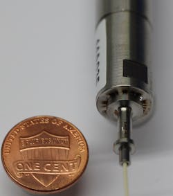
The coupling of blue laser radiation into a single-mode fiber without power loss requires a shift of the position of the parts of less than 0.1 µm (FIGURE 1). Building a multichannel sensor for space missions needs similar precision plus increased stability against shock and vibration and aligning a Stirling cooler are interesting examples that combine the need for minimized weld shift with gas-tight seam welding.
An extremely meticulous development not only from the provider of the production system, but also from the device designer enables stable manufacturing processes for such critical devices.
Why deformation?
Applying laser radiation with sufficient power density melts the metal and a liquid weld pool is formed. During cool-down, the metal volume shrinks, causing a deformation. Such a miniature deformation can produce a misplacement of two parts that have been aligned to a perfect position prior to the welding procedure.
Introduction of laser energy
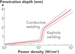
For most shift-sensitive devices, mechanical stability is less important than maintaining position during the welding with low shift. Therefore, conductive welding is preferred, as it requires less optical power between 500 kW/cm² and 1 MW/cm² compared to keyhole welding, which has substantially higher specific power well in the range of several megawatts per square centimeter. With conductive welding, the laser beam penetrates approximately as deep into the material as its diameter on the target.
In most cases, solid-state lasers producing a beam around the 1.06 µm wavelength are used for the welding operation of metals (FIGURE 2). The power generated in the laser resonator may be optically split into two or three beams with a uniform power level. The number of simultaneous weld spots is chosen according to the device geometry so that the laser energy will be introduced symmetrically.Typically, a power of less than 1 kW over a duration of 2 to 3 ms per weld spot with 300 µm diameter provides optimal results. The optical power needs to be adjusted between the beams with a deviation of less than 1% for critical applications.
Types of weld joints
A couple of configurations can be chosen for welding two pieces together. In any case, the two weld surfaces should form a close contact without gap in order to minimize the required weld energy.
Fillet welding is most suitable for laser welding with minimal shift. A laser beam is directed to the contact line of the two workpieces under an angle of 45°. As the workpieces form a corner of 90°, a small deviation of the position of the two pieces has no impact on the shift. In this configuration, the smaller workpiece should have no chamfer, as the laser beams will be unevenly absorbed form the two workpieces. The incidence of the laser beam allows for repeatable conductive welding.
Penetration welding requires perfect contact between the two pieces. An air gap would impede the melting pool and, consequently, the penetration in the lower workpieces would be negatively affected. Penetration welding needs larger peak power, which leads to larger weld shift.
Butt welding is not appropriate for low-shift precision welding. The mechanical tolerances of the two parts make it nearly impossible to maintain a repeatable geometry for each weld spot.
Device design
The design of the workpieces should follow a few simple rules. First, the material of the two pieces should be suitable for laser welding. Most stainless steels with low content of sulfur and carbon, Kovar, and nickel are suitable materials. Gold plating should be avoided, as it flows into the welding pool and results in microcracks that impair the gas tightness and mechanical stability.
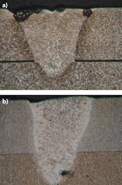
The laser beams need unobstructed access to the weld positions, which should be arranged in a symmetrical geometry. The laser beams must always hit full material—chamfers or other recesses have to be avoided (FIGURE 3). Perfectly flat welding surfaces avoids warping of the parts during the assembly.Design of manufacturing system
The production system for low-shift welding provides stable and repeatable fixing of the parts to be joined. In most cases, an active alignment process with a resolution of 20 nm is executed before the laser welding for final assembly.
In order to achieve the best result, two, three, or even more weld beams are used. This configuration serves for a homogenous and balanced application of the laser energy.
For workpieces with a circular shape, three weld beams under an angle of 120° to each other offer the best performance. This geometry allows for the lowest shift welding processes.
For planar workpieces, two weld heads are sufficient. These are oriented symmetrically along the device axis. The aim is to avoid tombstone effect—that is, tilting of the workpiece if only one beam is used.
Weld optic with CCD camera
The weld optics focus the laser beam down to a spot size of 200 or 300 µm. Larger spot sizes are seldom used, as the objective is low-shift welding and large weld spots that require higher overall energy are not beneficial.
The weld heads work with a collinear CCD camera. The different focal planes of the visible spectrum and the infrared weld beam are corrected. During the adjustment process, a sharp image from the camera indicates that the weld head is adjusted to its correct focal position.
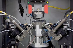
Additionally, a projected crosshair will be centered to the weld spot position so that it superimposes perfectly with the laser beam (FIGURE 4).In this way, machine vision algorithms can be used for automated and correct adjustment of the weld optics in space—both for focus and hitting exactly the border between the two parts to be joined.
Laser welding should always occur in the waist of the beam with a precision of 10 µm in order to keep the power density constant. If the beam on the target is out of focus, the power density changes rapidly and an uneven weld pool is generated.
As firm contact between the welding surfaces is one of the key factors for low-shift welding, the machine design needs to comply with this important factor.
A proven technique for adjusting cylindrical parts to best parallelism is a dome-shaped air bearing. The parts are moved in contact with a preset force and will self-adjust as one of the parts floats on an air bearing. Once the surfaces are adjusted for parallelism, the angular position is frozen and an active alignment can take place. Alternatively, a gimbal mount design adjusts the two parts.
In a planar setup, predetermined offsets compensate for the anticipated weld shift. The better the tolerance of the parts, the more accurate this corrective offset can be set.
Correcting weld shift
If a welded workpiece exhibits shift during the nanowelding process, a further application of weld energy at an opposite location bends the part back into the desired position. In this process, the effect of the inevitable shrinkage is used. To determine the right amount of power and time of the corrective laser pulse, it requires careful experimenting until the optimal parameters are found. This process is called laser-induced micro adjustment (LIMA).
Forming weld joints for nanostructures requires a design of the parts that is optimized for laser welding. The welding system has to take the specific aspect of the part into account. It is advisable that the designer of the nanostructures and the welding system manufacturer work together from start of the project to obtain an optimal result.
GUENTER HUMMELT(guenter.hummelt@nanosystec.net) is the CTO of nanosystec GmbH, Gross-Umstadt, Germany; www.nanosystec.com.


