Microstructuring with ultrashort-pulse lasers: Faster or smoother?
So far, it is well known that ultrashort-pulse (USP) lasers can reach highest precision in microstructuring, but they are too expensive, too slow, or just too exotic. That may change with the new generation of high-power USP lasers. With average powers of 100 W or more, they enable more throughput while maintaining their precision. That is good news for the tooling and mold industry, where steel tools have to be processed with very high precision.
Still, finding the right settings for USP lasers requires some understanding of processes and laser parameters. With the right parameters, you can turn more USP power into higher efficiency until they ablate even more than a nanosecond laser does. To find out more about optimum settings for USP laser processes, experts at the Fraunhofer Institute for Laser Technology (Fraunhofer ILT; Aachen, Germany) compared microstructuring results from nanosecond lasers with those from picosecond lasers. They found that the USP lasers can be 4X faster or they can reach a 4X smaller surface roughness with similar efficiency, if the right process parameters are chosen.
Further, the experts developed optimized parameters to use USP lasers for different processes such as cleaning and polishing. That allows for a dedicated photonic process chain where the same laser system can be used for subsequent tasks such as ablation, cleaning, and polishing. This way, the USP laser leaves its niche and becomes a very handy tool for various tasks in modern industry—it finally arrives on the shop floor.
Comparing picosecond and nanosecond pulses
It seems obvious that higher average power means higher ablation rate. For USP lasers, this is only partially true. As discussed earlier in this magazine,1 there is an optimum fluence (pulse energy per spot area) at about 7X the threshold fluence. Higher energies per pulse do not lead to higher ablation rates per second, and they may generate rough surfaces with cone-like protrusions. A viable solution for this problem can be the application of multibeam optics, directing the energy of one pulse into many similar beamlets.2
The other way to exploit higher average power would be higher repetition rates with moderate pulse energies—this poses challenges for the scanner technology, which have yet to be mastered. A much simpler solution for many purposes is the use of bursts, which uses conventional galvo scanners. A burst is a sequence of several equal laser pulses, separated by a few nanoseconds. The power of a burst is then the sum of the single pulses’ powers. Bursts are repeated at the regular repetition rate of the laser of typically some 100 kHz. More details of USP bursts can be found elsewhere.3,4
The actual advantage of USP lasers is their processing precision. They can ablate with submicron accuracy and almost without heat-affected zones. Once higher average power USP lasers are available, the crucial question is, can these advantages be maintained at higher throughput rates? To answer this question, scientists at Fraunhofer ILT have compared the ablation processes of USP lasers and of nanosecond lasers.
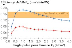
For benchmarking, a fiber laser with 400 ns pulse duration and variable pulse energies was used. It was compared with a USP laser with pulse lengths of 2 ps and 10 ps in single-pulse mode (FIGURE 1). By reducing the pulse duration from 10 ps to 2 ps, the efficiency increases by a factor of about 2.5. With this improvement, the USP laser is able to ablate as many volumes per minute and watt as the 400 ns laser. The 2 ps laser ablates more than 40 mm3 steel per minute at an average power of 312 W. Interestingly, the 10 ps pulses reached only about 30% of the ablation per watt and minute. This demonstrates that USP is not equal to USP—after all, FIGURE 1 shows that a USP laser with pulses as short as 2 ps can ablate as much or more material than a nanosecond laser.
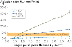
Now, what happens if bursts of laser pulses are applied? FIGURE 2 shows how the ablation rate increases with the number of pulses per burst and with the applied fluence per pulse. All pulses in a burst contribute to ablation, so more pulses per burst lead to a higher ablation per burst.For example, in single pulse operation with a fluence of 1 J/cm2, the USP laser (2 ps) achieved an ablation rate of 1.49 mm3/min. With 10 pulses per burst (PpB), the same laser achieved 10.15 mm3/min. With a fluence of 4 J/cm2, the system even reached 42 mm3/min. The maximum applied power has been 312 W at a repetition rate of 500 kHz.
Finding the sweet spot
There is an obvious question resulting from these observations: What happens to the surface quality if the number of pulses is increased? The short answer is, it depends. The surface quality improves when we go from one to five pulses per burst, but it gets worse for 10 pulses per burst.
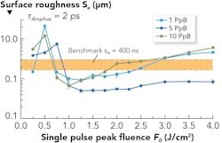
FIGURE 3 shows measurements of the surface quality in ablation experiments on a steel surface using a 2 ps laser. Again, the fluence has been increased stepwise and data has been taken for different bursts and compared to the roughness achieved with a nanosecond laser. It should be noted that the fluence here refers to every single pulse. Accordingly, much more energy is deposited during a burst.It turns out that the roughness from the USP ablation is larger than from the nanosecond laser for small and large fluences for very low and high numbers of pulses per burst. In between, there is a sweet spot, where the surface roughness for the USP laser ablation goes down to 0.5 µm.
After all, these results show that the USP laser allows for two different processing strategies:
High ablation rate. With bursts of up to 10 pulses and fluences of up to 3 J/cm2, the USP laser can achieve an ablation rate that is 3–4X as high as from the nanosecond laser. The surface roughness can be kept at similar levels.
Low roughness. With fluences between 1 and 2 J/cm2 and five pulses per burst, the surfaces can be made much smoother (down to 0.5 µm) while retaining the same ablation rate as with nanosecond lasers.
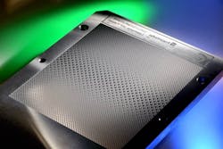
Of course, this depends on the actual material used; these tests were done on steel 1.2738, a material that is often used for mold tools as applied in the fabrication of plastic parts. FIGURE 4 shows several examples, where the USP laser has been used for microstructuring of steel tool surfaces. The ablation rate for the average power of 90 W (5 PpB) was similar to the ablation rate of a nanosecond laser. At the same time, the surface was much smoother.For higher average power of 165 W and similar burst settings, the ablation rate doubles to about 20 mm3/min, while the surface roughness doubles to 1.3 µm (pyramid structure) or 1.5 µm (carbon-tex structure). A typical industrial nanosecond laser achieves a roughness of 1.5 µm at 5 mm3/min or 2.5 µm at 10 mm3/min. So, the USP laser at 165 W can ablate 4X as much material as the nanosecond laser at similar surface qualities. Or, with lower power, it achieves a 4X lower surface roughness at similar ablation rates.
Cleaning and polishing with USP lasers
Microstructuring is a process that benefits from the precision of USP lasers. The processes rely on the extremely short interaction of these lasers. In cleaning processes, for example, ultrashort pulses blast away oxide layers from surfaces. With proper settings, this cleaning process happens almost instantaneously without melting the actual surface.
Polishing is a different process where the surface is locally molten to flatten the surface on that spot. Depending on the size of the unevenness, the surface can be heated to different degrees. Obviously, cleaning and polishing require different sets of process parameters. In the polishing process, for example, these parameters must not exceed the fluence threshold for ablation.
Understanding the processes helps to find appropriate parameter spaces. For cleaning, a rapid process without heat accumulation is needed. Thus, single pulses with a fluence just above the ablation threshold will do the job.
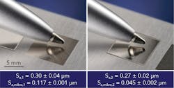
For polishing, heat accumulation is desired. Therefore, a long burst with low energy pulses will be well suited. Their added fluence must not exceed the ablation threshold. So, the energy of the individual pulse within the burst is kept much lower than for cleaning. The scanning rate also has to be adjusted, as it may need several bursts on one spot to get the surface molten.Different surface structures need different polishing processes. For example, a roughness of about 1.0 µm may need another treatment than a roughness of about 0.5 µm. FIGURE 5 shows the success of a USP laser polishing process (a) where the initial grinded surface is smoothed from initially 0.6 µm to 0.3 µm. A more detailed and scientific view on the quite-new approach of USP polishing is available.5
Fast processing of smooth surfaces with a photonic process chain
So far, it has been shown that on the one hand, USP lasers can ablate faster or smoother than nanosecond lasers. On the other hand, USP lasers can be used for cleaning and polishing surfaces. Together, this knowledge can be used to establish a fully photonic process chain where rapid USP ablation is followed by a cleaning step and, finally, a USP polishing procedure. Researchers at Fraunhofer ILT found that the total USP process is still 14–59% faster than a comparable nanosecond laser ablation. At the same time, the surface roughness is about 0.17 µm, which is about 90% better than the surface from the nanosecond process.This integrated photonic process chain offers various benefits for the tool and mold industry—for example, it can be implemented in five-axis machines. Typical application cases are in the automotive industry, where tools for plastic parts in a car interior can be processed with this method. As a test, a sample tool for Volkswagen has been processed with USP lasers in a three-step process chain consisting of structuring, cleaning, and polishing (FIGURE 6). The sample has been made in one machine with one clamping. In similar processes with nanosecond structuring, the workpiece has to be reworked. The processing time is kept constant with USP lasers while achieving a surface roughness of 0.5 µm on the non-polished areas (4X lower than with the nanosecond process).
This research has been executed within the project eVerest. It has been funded by the German Federal Ministry of Research and Education (BMBF).
REFERENCES
1. N. Hodgson et al., “Industrial femtosecond lasers and material processing,” Industrial Laser Solutions online (Jan. 2019); https://bit.ly/HodgsonRef.
2. J. Finger and A. Thoss, “High-throughput ultrashort-pulse laser micromachining,” Industrial Laser Solutions, 21-23 (Jan/Feb 2020); https://bit.ly/MicrostructRef2.
3. J. Finger et al., Adv. Opt. Technol., 7, 3 (May 2018); https://doi.org/10.1515/aot-2018-0008.
4. A. Brenner, B. Bornschlegel, and J. Finger, J. Laser Micro. Nanoen., 14, 1, 100–107 (2019); doi:10.2961/jlmn.2019.01.0017.
5. A. Brenner, L. Röther, M. Osbild, and J. Finger, Proc. SPIE, 11268, 112680P (Mar. 2, 2020); doi:10.1117/12.2551481.
About the Author
Andreas Thoss
Contributing Editor, Germany
Andreas Thoss is the Managing Director of THOSS Media (Berlin) and has many years of experience in photonics-related research, publishing, marketing, and public relations. He worked with John Wiley & Sons until 2010, when he founded THOSS Media. In 2012, he founded the scientific journal Advanced Optical Technologies. His university research focused on ultrashort and ultra-intense laser pulses, and he holds several patents.
Andreas Brenner
Team Manager, Thin Film Structuring at the Fraunhofer Institute for Laser Technology
Andreas Brenner is Team Manager, Thin Film Structuring at the Fraunhofer Institute for Laser Technology (Fraunhofer ILT; Aachen, Germany).
