Applied research pushes the deployment of laser technologies
KAROLIS RATAUTAS, PAULIUS GEČYS, MINDAUGAS GEDVILAS, and GEDIMINAS RAČIUKAITIS
On its 60th anniversary, the fields of laser application, particularly in material processing, are expanding steadily, and most of the advanced solutions come with the use of ultrashort-pulse (USP) lasers, a type of laser for which Lithuanian companies are well recognized globally.
The Department of Laser Technologies at FTMC – the Center for Physical Sciences and Technology (Vilnius, Lithuania) is one of the active places in Europe where new technologies and applications for lasers are born. The following is a review of the department’s recent high-maturity level developments ready to be directly installed by customers.
Glass processing technologies
Novel laser glass processing techniques, offering high speed and precise fabrication, have become an attractive alternative to conventional methods, such as mechanical dicing, diamond saw, and waterjet cutting. With the evolution of modern industrial lasers, laser-based technologies are ensuring high throughput as well as higher quality.
One of the most flexible glass processing techniques is laser rear-side processing. The process is initiated by focusing the laser beam through the glass sample to the back surface of a transparent substrate. It is a very efficient process that could reach >120 mm3/min material removal rate with a laser emitting just 20 W. Utilizing this technique, the typical kerf width can be remarkably reduced compared to mechanical diamond tool processing. Therefore, feature sizes as small as 150 µm can be laser-machined. The laser cuts are taper-less, and it is feasible to fabricate extremely high-aspect-ratio features. Excellent cutting quality can be obtained with surface chipping <50 µm, and the chamfering process also can be realized. The method was validated on float glass, borosilicate glass, and fused silica. The process is accomplished via galvanometer scanner beam positioning—therefore, there are almost no process shape restrictions. Furthermore, process stitching is implemented to extend the fabrication field to industrial requirements.
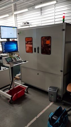
FIGURE 1 presents the laser system for glass processing working in the production of displacement and rotation encoders.
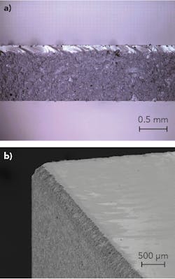
Laser rear-side processing is a very flexible technique. However, some applications require extremely high-throughput cutting of straight lines of simply shaped contours. The most efficient laser-based kerf-less method is dicing by introducing intra-volume voids, followed by a mechanical separation step. In order to perform predicted separation, elongated modifications ranging through the entire glass thickness needs to be generated. For this, the modified Bessel optical beams are used in such applications due to large nondiffractive length. Glass dicing is a very efficient process and up to meters-per-second dicing speed can be obtained with glass thicknesses ranging from a few hundreds of microns to a few millimeters (FIGURE 2).The focused laser beam can be applied not only for cutting and drilling, but 2.5D milling processing is possible as well.
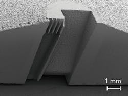
An exciting emerging field of application for the technique is the fabrication of gas injection nozzles. Gas nozzles are used in various laser-plasma experiments for laser wakefield acceleration (LWFA), secondary x-ray, and γ-light generation toward industrial tomography and medical treatment applications. Tailored plasma targets require the implementation of the complexed-shaped nozzles with converging-diverging and cylindrical throats to get modulation of gas concentration along to the laser beam propagation. Such complex shapes are complicated or, in many cases, impossible to produce with conventional techniques. Further, the channel wall roughness has a crucial impact on the nozzle performance, and fused silica is much more resistant compared with metals. The Department of Laser Technologies has developed a hybrid laser processing technique, where nanosecond laser processing is combined with the femtosecond laser-induced selective etching (FLISE) technique (FIGURE 3). Such a unique combination allowed us to reach high submicron-scale resolution together with high-speed material processing.1Precise and high-efficiency laser ablation
Nature-inspired surfaces and their replication are getting a huge amount of interest in science, technology, and medicine due to their unique functional properties. Particular attention is paid to surfaces that replicate the shark-skin texture, which reduces friction with liquids or gases and has antibacterial properties. Our team at FTMC has developed an efficient laser-ablation technology, keeping a maximal material removal rate together with ultimate processing quality. The technology was validated by replication of shark-skin-like structures over large areas at high speeds.
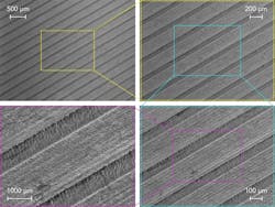
Findings of the theoretical way to predict an optimal set of processing parameters for the most efficient laser ablation advanced in the readiness level of laser milling technology to real use in biomimetical applications. Achievement of the highest-known laser milling ablation efficiency for copper, using a state-of-the-art bi-burst femtosecond laser,2 together with the minimal roughness of the laser-milled surface and best machining quality,3 the new laser technology is advanced over its competitors. The friction with air, of laser structured shark-skin-like surfaces studies, showed a drag-force decrease by up to 6%. The ability to mimic the bio-inspired surfaces of shark skin-like structures, drag-reducing trapezoidal-riblet structures (FIGURE 4), and fish scale-like structures or other complex tree-dimensional shapes at high fabrication speed while maintaining lowest-possible surface roughness has enabled the efficient laser ablation technology to successfully compete with conventional industrial techniques.The optimized and controlled laser beam scanning procedure is a flexible and reliable technique to replicate a broad diversity of functional surfaces naturally developed in nature. The increasing ultrashort laser power with decreasing price-to-power ratio, together with the development of efficient and precision laser milling technology, opens new opportunities for real commercialization of bio-inspired functional surfaces starting from small-batch laboratory production to large-scale industrial applications in the very near future.
Combining laser and chemical technologies
Fabrication of circuit traces is the most challenging task for in-mold integrated electronics production, called 3D-MID (Molded Interconnect Devices). It is both technically difficult to achieve and challenging to make cost-effectively. MID is an injection-molded thermoplastic part with electronic circuits directly integrated into a polymeric component. It offers material, weight, and cost savings by the elimination of connectors between separate printed circuit boards, shortening the process chain and integration of contact surfaces in, for example, switches, sensors, and antennas. MID has a great potential in automotive, aviation, lighting, computing, or even medicine sectors, where emerging innovation demands an increase in the number of the electronic components into a device. However, a standard well-known technique such as photolithography could not be applied in a conventional way since the parts generally have complex 3D geometrical shapes. We have developed a new method called Selective Surface Activation Induced by a Laser (SSAIL), which is a promising technology for solving challenges in the production of electrical conductors on polymers.4 SSAIL contains three main steps: laser modification of the dielectric surface, chemical activation of the modified areas by dipping into a solution, and chemical electroless metal deposition of the activated parts. The new technology offers laser writing speeds of up to 4 m/s, and herewith spatial plating pitch is kept as narrow as 25 µm.5
The main advantages of the SSAIL process compared with other technologies (like laser direct structuring) is that SSAIL does not require special additives in the polymer matrix and standard commercial material (available on the market) can be used as a circuit carrier. Therefore, SSAIL could open a broad area of application where current methods of electronics integration are still too expensive. Additional advantages are related to SSAIL capability to process transparent and flexible polymers (FIGURE 5).Digital transformation of the industry
Digital transformations are moving through all branches of industry in all countries. Even during the COVID-19 outbreak, ideas for state support are about high and advanced technologies businesses. For laser technologies, that is an excellent opportunity.
FTMC, together with our science park and the cluster of laser and engineering industry technologies, LITEK, are running a Laser LT Digital Innovation Hub, with the intention of helping local companies in the transformation of their production routes utilizing laser and other photonic technologies. For us, that is a chance to promote new developments and deploy them on the factory floor.
Furthermore, a new European Horizon 2020 project called PULSATE on laser DIH was just signed to start support for companies in the easier and faster adaptation of laser technologies in their production at the European scale.
REFERENCES
1. V. Tomkus et al., Appl. Surf. Sci., 483, 205–211 (2019).
2. A. Žemaitis, P. Gečys, M. Barkauskas, G. Račiukaitis, and M. Gedvilas, Sci. Rep., 9, 12280 (2019).
3. A. Žemaitis, M. Gaidys, P. Gečys, G. Račiukaitis, and M. Gedvilas, Opt. Lasers Eng., 114, 83 (2019).
4. K. Ratautas, A. Jagminienė, I Stankevičienė, E. Norkus, and G. Račiukaitis, Appl. Surf. Sci., 470, 405–410 (2019).
5. K. Ratautas et al., Results Phys., 16, 102943 (2020).
KAROLIS RATAUTAS, PAULIUS GEČYS, MINDAUGAS GEDVILAS, and GEDIMINAS RAČIUKAITIS ([email protected]) are with the Center for Physical Sciences and Technology, Department of Laser Technologies, Vilnius, Lithuania; https://lts-ftmc.lt.


