ANDERS PENNEKENDORF
Whether for cutting, scribing, drilling, or structuring, lasers are being used for many different applications. While laser material processing must be quick and precise, it also must maintain a high production throughput—therefore, integrating a laser into a manufacturing process poses several challenges. The laser industry is regularly developing innovations to further optimize production processes and ensure that components are high-quality.
Having been around for only 60 years, the laser is still a relatively new technology. Albert Einstein laid the foundation for modern laser technology with his principle of stimulated emission in 1917, but it was U.S. physicist Theodore Harold Maiman who developed the first laser in 1960, which proved to be one of the defining inventions of the 20th century. Laser technology became an industry standard in the 1970s and to this day, laser separation boasts greater flexibility, controllability, and above all unparalleled quality in comparison to mechanical processes.
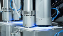
Components are becoming ever smaller and more filigreed, and the processing must be correspondingly fine and precise. That is why a guaranteed level of quality and accuracy are especially important in micromaterial processing. This is where the laser truly shines over conventional and mechanical processes, such as sawing or milling, because design features can be adapted quickly, eliminating the need to rework products in the production process. Another decisive point is the fact that laser processing is compatible with a variety of materials, including metals, such as aluminum, stainless steel, iron, and titanium, and non-metals, such as plastics, composite materials, and ceramics (FIGURE 1).
Applications of electronic components
High-performance ceramic materials have become indispensable in micro- and precision engineering and are used in a wide range of applications as substrate materials due to their electrical, mechanical, and thermal properties. This is true for the production of modern electronic components, for example, where ceramics are used as a carrier material.
These components are used in the drive controls of electric vehicles, in automotive components, and in power engineering. They are made using direct bonding copper (DBC) substrates, which consist of copper-ceramic compounds with mostly aluminum oxide or nitride acting as a layer of isolation and copper compounds making up the electrically conductive layout.
The increase in electric car production in particular is driving the demand for high-performance batteries. High-energy currents have to be transmitted within a very short time and fast electrical switching processes must be made possible. These requirements affect the demands made on the quality of the electrical connection: the more complex the battery set, the more complex the electronic components.
Ceramics in laser micromaterial processing
However, using ceramics as a processing material also has its disadvantages, which have already been demonstrated by conventional processing methods. The material is inherently very brittle, making it difficult to cut or drill with sawing or milling techniques without causing cracks or stresses in the substrate. Its disadvantages are obvious: material can only be processed at lower speeds, milling heads and saw blades wear out, and the operating costs are relatively high. In addition, ceramics often need to be reworked to maintain quality standards.
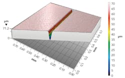
Using lasers to process ceramics has its advantages. This is where laser scribing techniques have proven successful. Historically, it was precisely this application that established the laser as a reliable processing tool in the industrial environment. Even today, ceramic scribing by laser is still considered a cost-effective and widely used manufacturing application. Using conventional laser scribing methods on ceramic substrates generates a defined break line in the substrate, which facilitates a clean and precise separation into individual segments. They can then be separated by a machine or manually (FIGURE 2).For a long time, carbon dioxide (CO2) lasers were primarily used for laser scribing. This laser works with a power range of up to 250 W continuous-wave (CW) with a wavelength between 9.4 and 10.6 µm. Because they produce a large amount of heat, there are common undesirable side effects, such as melting beads, material throw-up, glazing, and microcracks in the substrate. The same disadvantages apply to other methods that make use of solid-state lasers, the pulse widths of which are in the two-digit nanosecond range.
Using ultrashort pulse (USP) lasers for processing allows burr-free scribing lines to be created in the substrate and thermally induced material stresses to be reduced through a cold ablation process. The short pulses in the range of 10 ps to 200 fs result in a high pulse peak power, which acts on the workpiece due to the high repetition rate and transfers the material directly from a solid to a plasma-like aggregate state. There is also flexibility in the choice of wavelength, as USP lasers are available in the common wavelength ranges 1064 nm (infrared), 532 nm (green), and 355 nm (ultraviolet), and have become established in industry.
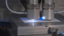
As the breaking edges are so precise, microcracks are not introduced into the substrate and spontaneous break does not occur. This results in a continuous, 20–70 µm deep, burr-free kerf, which guarantees high quality and accurate separation of the ceramic circuit boards. Production throughput is increased as a result of the ceramic circuit boards’ higher breaking strength. In addition, the USP laser process produces significantly less machining residue than the conventional CO2 method. This greatly reduces or even completely eliminates any subsequent cleaning steps (FIGURE 3).Ultrashort-pulse lasers have also proven to be useful in other processes, such as drilling, cutting, and creating cavities. In all these processes, material ablation takes place layer by layer. During this process, the substrate is either completely cut through or the material is ablated to a predetermined depth. The use of suitable laser sources with pulse lengths in the picosecond and femtosecond range guarantees high surface quality with minimal thermal stress on the material.
When laser cutting ceramic substrates, any geometry with minimal radii can be generated in the substrate. This applies to both internal and external contours. Laser drilling, on the other hand, allows for incredibly small hole diameters. Depending on the diameter of the hole, trepanning, or percussion drilling can be used to produce the ideal geometries. Cavities—that is, depressions in the substrate—can also be created by targeted material removal. This enables, for example, microchips or resistors to be embedded. The laser process allows precise control of the ablation depth and geometry of the cavity.
Besides ceramic substrates and ceramic circuit boards, cutting, drilling, and scribing process techniques can also be applied to electrical circuit boards. One specific process for separating segments is called depaneling.
Depaneling printed circuit boards
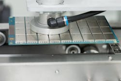
Laser cutting technology for depaneling, currently available on the market, is one of the most innovative processes for separating printed circuit boards (PCBs) from a whole panel. In contrast to conventional or mechanical milling and sawing processes, laser depaneling separates the panels from each other without any external contact. The separation is instead achieved by ablating the material with the laser layer by layer. Contact-free processing technology is particularly lucrative for companies because it is delicate on both the material to be processed and the laser itself. Since wear and tear is extremely low, operating costs are reduced while quality remains a guarantee in the long-term. Full Cut technology allows for up to 30% more space utilization as the panels fit together seamlessly when cut by a laser. There is also no excess material left behind after processing, which also reduces costs (FIGURE 4).A look ahead
For many years, CO2 lasers dominated the cutting and scribing market before USP technology came about. The increasing demand for ever-finer and higher-quality electronic components has a considerable influence on the requirements of the entire PCB industry. Just think of LEDs, smoke detectors, or MP3 players. Several new laser technologies have been developed and implemented to meet this challenge in recent years. There is potential for laser-based processes in the growing market for flexible electronics. This will require a quick and easy way of structuring thin layers on flexible substrates, offering room for innovative laser manufacturing processes.
ANDERS PENNEKENDORF([email protected]) is Senior Sales Manager at Photonics Systems Group, Krailling, Germany; photonics-systems-group.com.


