3D-Micromac enters collaboration to increase efficiency of failure analysis workflows

Laser micromachining systems maker 3D-Micromac (Chemnitz, Germany) has joined forces with scientific instrumentation developer TESCAN (Brno, Czech Republic) to provide a more efficient workflow to diagnose a variety of materials and to root cause defects in functional materials and devices. The work aims to reduce the labor and time cost to reach the region of interest (ROI) in minutes.
Currently, samples of metals, semiconductors, ceramics, and compound materials are analyzed with focused ion beam (FIB) methods. TESCAN’s Plasma FIB-SEM scanning electron microscope is used throughout the semiconductor, automotive, and aerospace market segments as an industry-proven solution. These have, however, an increasing need for even larger volume material removal when failure analysis (FA) is required on deeply buried ROIs or very large cross-sections.
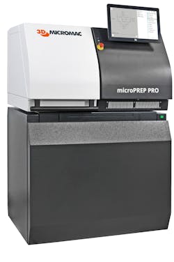
TESCAN and 3D-Micromac can decrease the time-to-result of demanding FA tasks, with the ability to analyze even larger volumes and create a much more productive workflow for industrial FA environments. For example, typical sample preparation with the Plasma FIB-SEM can take several hours and is mainly focused on FA tasks of submillimeter dimensions. 3D-Micromac’s microPREP PRO laser micromachining system uses an ultrashort laser pulse ablation technique that allows the processing of much larger volume tasks in FA exceeding a cubic millimeter.
The current application solution is already reducing the FA time in most tested cases at least by 50%, in some applications even 95%. On average, 75% of the overall time is saved by using TESCAN’s Plasma FIB-SEMs together with 3D-Micromac’s microPREP PRO flexible laser systems. Further joint development will ensure that Plasma FIB-SEMs and microPREP PRO systems do not act as individual instruments, but become an integral part of the FA lab ecosystem.