Laser processing technologies in the PCB industry
Today, some manufacturers still consider laser processing technology as relatively new, and this has catalyzed the growth and need for laser processing technologies to provide high-quality products over the decades. The use of laser technology in the printed circuit board (PCB) industry is seen as critical in technological advancement with cutting-edge innovation that ensures practical and stylish electronic devices. By incorporating laser processing technologies, the PCB industry is gradually taking charge and rising above the traditional processing technologies used in the electrical industry.
Mainstreaming HDI laser processing techniques
Over the years traditional electronic manufacturing technology is increasingly becoming unsuitable, more so in high-density interconnection (HDI) structures. These conventional electronic manufacturing technologies have lower yields, expensive production, and limited flexibility. To ensure the HDI structure and PCBs are helpful and in line with the rapid technological advancements, manufacturing companies need to embrace the use of laser processing technology. But with technology companies embracing HDI processing, PCB multilayer industries produce better resolution devices and provide versatility in manufacturing processing and fast processing speeds.
The case for CO2 lasers
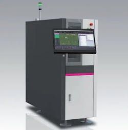
The manufacture of PCBs involves the drilling of microvias (small holes) that allow electrical connectivity between the layers in the circuit boards. To successfully achieve this precision, manufacturers have for years used carbon dioxide (CO2) lasers (see Fig. 1). Unfortunately, the use of CO2 has in recent years decreased to currently servicing about 20% in the PCB industry. CO2 laser technology showed efficiency in removing dielectric, even nonuniform glass dielectric, in the two decades of use. But CO2 lasers cannot remove copper or drill holes less than 75 μm in diameter. On the other hand, ultraviolet (UV) lasers can drill small holes and even remove electro copper foil. The increasing need for more refined and high-quality electronic equipment has led to the slow rise in the use of CO2 laser technology. There is a need for CO2 laser technologies to improve and work on providing innovative laser technology to meet ever-growing electronic innovations.
This does not discredit the use of CO2 lasers. On the contrary, CO2 laser technology is expanding, creating a stronghold in the PCB industry—but to ensure manufacturers get the best, the UV laser is more effective. The UV laser, while effective in the PCB industry, has a few shortcomings. UV laser technology can erase dielectric material, but it is slow and doesn’t provide consistent results on glass-reinforced material. This use of a hybrid laser drill system with both UV and CO2 lasers provides the best results, with the CO2 laser providing fast drilling and UV laser drilling on small holes and copper foil.
Mechanical via drilling
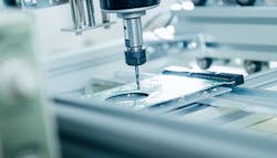
The evolution in the manufacture of electronic devices for the past few generations has focused a lot on making electronic designs smaller and thinner. This means the PCB industry has had to make similar changes in their designs. However, mechanical drilling has a lower upfront cost and has the strength to drill through several boards (see Fig. 2). The downside in using mechanical drills is that they lack precision and require frequent maintenance after a few hundred vias, which subsequently affects the cost of ownership. However, an increase in the use of HDI processing technology has led to a decrease in the size of the vias, enabling one PCB to hold more microvias. These limitations in using a mechanical drill has led to the introduction and wide use of laser processing technologies.Cost of ownership considerations
The scales in the running and cost of ownership are tipping towards the use of laser technology in the PCB industry. The growth in this technology has played a significant role in widespread use and facilitated multilayered PCB industries’ move to HDI processing technologies. Laser technology in the PCB industry is a highly innovative method and has managed to reduce wastage, increase efficiency, and thus this affects the cost of ownership. For the PCB industry to grow while providing the best for its clients, it is essential to cut costs, and the use of laser technology has had a significant impact on this growth.
With the cost of ownership considerations, companies in the PCB industry can accurately assess any direct or indirect costs affecting the running of the business. With its high-end and cutting-edge technology, use of laser technology reduces waste, is fast, and can be used to perform various tasks in the industry. Additionally, laser technology has reduced wear and tear, allows space utilization, and maintains high quality in the PCB sector.
The ever-changing technological advances challenge the PCB industry to address electronic market trends by providing efficient advanced designs without adding cost. The best way for the PCB industry to achieve this is by fully embracing laser processing technologies.
Materials and market
There are various factors that are essential in the laser selection process. For instance, although the automotive industry is shifting to HDI and laser via processing for miniaturization purposes, there is a primary emphasis on design for reliability. High-frequency PCBs are in high demand, and regular FR4 materials are not ideal for use in this type of board. UV-based systems and other cutting-edge technologies are more suitable for use in this application, where the materials for use are not as limited.
Conclusion
There is a growing market for innovative electronics—this growth in the market has also led to the need for high-quality electronics. This growth has influenced the dominance of laser technology, and as manufacturers move towards thinner, sleek, and higher quality designs, so will the increase of laser technology. And as more developments in technology continue to create room for growth, it is crucial for laser technology manufacturers to work closely with other innovators to create a balance between PCB and electrical innovation with processing technologies.

