Cost, quality, and throughput are major factors in achieving successful manufacturing in the semiconductor and photovoltaics industry. One important process type is cutting, as different kinds of cutting processes are needed to separate wafers into dies or cut solar cells into half-cells. Traditional cutting techniques are mechanical- or laser-based, both of which are connected with disadvantages such as particle generation because of material removal and material damages at the cutting edge.
Thermal laser separation
Thermal laser separation (TLS-Dicing) is a fast, clean, and cost-effective alternative to separate brittle semiconductor materials such as silicon (Si), silicon carbide (SiC), germanium (Ge), and gallium arsenide (GaAs).
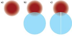
Depending on the application, a starting point is given by an initial scribe. Afterwards, the material is heated by a laser with a well-defined energy insertion (FIGURE 1a). The heated material expands and pressure forces occur inside the heated zone, accompanied by tensile stress around the heated zone. Laser heating is directly followed by a cooling jet of extremely small amounts (below 10 ml/min) of deionized water spray (FIGURE 1b). This creates a second cooled zone near the first zone that induces a tangential tensile stress pattern. The resulting tensile stress in the overlaying region of both stress patterns opens and guides the crack tip through the material (FIGURE 1c).
TLS-Dicing has many advantages compared to traditional cutting technologies, including high separation speed; very smooth side walls free of chipping and micro-cracks and with superior bending strength; and low cost of ownership because of no tool wear and almost no consumables.
The process uses two laser sources—a short-pulsed scribing laser (532nm, or near-infrared [near-IR] wavelength) with a Gaussian beam profile for the initial scribe and the cleaving laser. The cleaving is realized by a 200W continuous-wave laser with a near-IR wavelength.
TLS-Dicing is a kerfless cleaving process, as almost no particles are generated by TLS itself. In comparison to traditional technologies, TLS-Dicing is a one-pass process that separates the whole thickness of the wafer at once.
Dicing of SiC devices
Because of its wide band gap, high mechanical strength, and high thermal conductivity, SiC is used in certain power device applications. These devices can operate at higher voltages, frequencies, and temperatures, as well as convert electric power at higher efficiency or lower power losses. At the same time, SiC is an extremely hard and brittle material (Mohs scale 9.2), which can create processing challenges.
Traditional dicing technologies have some disadvantages concerning process speed and dicing quality. Mechanical sawing suffers from low feed rate and high wear of the dicing blade, resulting in higher cost. In addition, blade sawing can result in chipping and delamination at the edge of the die. In comparison, laser ablation leads to a significant heat-affected zone, low edge quality, and micro-cracks. In addition, the ablation rate is very low and multiple passes are needed to separate the dies.
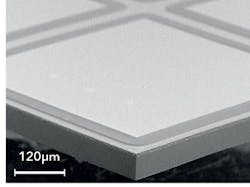
TLS-Dicing is a one-pass process that separates the whole thickness of the SiC wafer with a separation speed of up to 300mm/s. Since TLS-Dicing is a cleaving process, it has the potential to reduce the width of the dicing street and increase the number of chips per wafer. The die edges are smooth and free of remaining stress, micro-cracks, and chipping zone (FIGURE 2). Furthermore, metal structures in the dicing street on the front side, polyimide on the dies, and the backside metal can be separated with no delamination or heat effects.
Yield analyses on the use of the TLS-Dicing process on a typical power device wafer with full backside metallization, polyimide, and metal structures in the dicing streets have shown an average yield value >98%. In addition, TLS-Dicing has demonstrated a significant improvement in terms of cost per wafer [1]. 3D-Micromac's microDICE system using TLS-Dicing technology has already been used by major industrial manufacturers.
Cutting of Si solar cells
Cell separation has become industrially relevant because of the introduction of half-cell module concepts, which allow a substantial power gain. The standard industrial process of p-type cells is based on laser scribing and subsequent mechanical breaking. The disadvantages of this process are reduced cell efficiency and mechanical strength, as well as expensive handling because of the combination of a laser process with a subsequent mechanical breaking.
To overcome these drawbacks, 3D-Micromac is using TLS-Dicing in its industrial microCELL laser system for separating silicon solar cells into half-cells. Compared to conventional separation technologies, TLS-Dicing enables clean, micro-crack-free edges with no crystal damage on the separation edge (FIGURE 3). As opposed to laser cutting, no bulging and no formation of particles occurs because the substrate is merely heated and not vaporized. The mechanical stability of TLS-processed half-cells is significantly greater than conventionally processed solar cells.
TLS-Dicing allows feed rates of up to 500mm/s, resulting in an approximate 5X increase in the processing speed compared to conventional ablation and breaking methods. Laser processing on-the-fly and an innovative handling concept enable maximum throughput of approximately 10,000 half-cells per hour.
Current developments
Besides the use in photovoltaics or semiconductor industry, 3D-Micromac also offers a glass cutting process based on thermal laser separation. Here, the cleaving process is done using a CO2 laser. Depending on the application, a post-breaking or laser full-cut can be used.
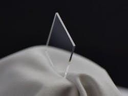
Cutting results comply with the requirements of industrial display production, and guarantee clean and gentle processing. Optically clear cutting edges free of micro-cracks can be achieved (FIGURE 4).
Focused applications range from microscope slides to covers for flat panel displays. The most commonly addressed glass types are soda lime in the 0.7 to 1.1mm range, as well as alkali-free boro aluminosilicate for flat-panel display applications from 0.1 to 0.7mm.
TLS-Dicing is a completely new approach to separating brittle semiconductor materials used in the semiconductor and photovoltaics industry at high throughput, low cost, and with high-separation quality. The cleaving is always a one-pass process. A feed rate between 300 and 500 mm/s applies, depending on the application. It produces excellent side-wall quality without chipping, and has a lower cost of ownership compared to traditional dicing or cutting technologies.
ACKNOWLEDGMENTS
TLS-Dicing, microDICE, and microCELL are trademarks of 3D-Micromac AG.
REFERENCE
[1] See https://goo.gl/h14mRh.
Mandy Gebhardt | Manager of Marketing and Public Relations, 3D-Micromac AG
Mandy Gebhardt is manager of marketing and public relations at 3D-Micromac AG (Chemnitz, Germany).


