Using tightly focused ultrashort pulses, reliable micro-welding can be achieved through almost all types of transparent materials, including polymers, dielectrics, or even ceramics. In this approach, the two materials to be joined are placed in contact. The top one must be transparent to the laser radiation so the beam can propagate through and allow focusing at the interface. Upon absorption, both materials will melt and join after resolidification, leading to the bonding of both top and bottom pieces.
This leads to a key additive manufacturing process applied in many technological and scientific domains from the assembly of optomechanical components to advanced encapsulation technologies for temperature-sensitive components (e.g., electronics). It is nevertheless striking to note an important exception in this picture. Despite their transparencies in the infrared (IR) domain of the spectrum, reliable joining of semiconductor materials was impossible using standard laser processing procedures.
It was accepted that this long-standing problem was due to the strong propagation nonlinearities in narrow bandgap materials that, in the case of beams focused below the surface, resulted in defocusing and pre-focal plasma formation. In the case of ultrafast IR light inside semiconductors, these phenomena prevented efficient energy deposition at the focal spot. This hindered any kind of material modification and, in consequence, impeded the melting and subsequent resolidification at the interface between the two pieces to bond.
To address this question, recent works proposed complex compensation procedures based on trains of pulses, hyperfocusing strategies, or reducing nonlinearities by using longer pulses. The later one allowed demonstrating ultrafast laser silicon-metal welding by using picosecond pulses, where the bottom material was metal, which improved energy absorption. But within the framework of laser welding, semiconductor-semiconductor welding remained out of reach by this type of optimization.
This was due to a second important physical limitation recently revealed by our work at the LP3 laboratory, a joint unit between the French National Center for Scientific Research and Aix-Marseille University. We discovered that contact imperfections between high-refractive index semiconductors lead to an air gap at the interface between the two pieces (see Fig. 1). This acts as a resonating optical cavity driving out the energy density from the interface. Coincidently, this corresponds to a situation where one has to actually fight against an interferometric configuration similar to the famous Fabry-Perot type interferometer invented more than a century before (1899) in our city.1
Silicon-silicon laser welding
On the basis of this new knowledge, the first experimental demonstration of silicon-silicon laser welding was achieved with a processing configuration to circumvent both limitations. This involved, on one hand, using nanosecond pulses instead of ultrashort ones to reduce propagation nonlinearities and, on the other, placing the two semiconductor pieces in the most intimate optical contact to avoid any gap. In this way, welding of uniform areas extending from micrometers up to several millimeters can be readily performed and a very high bonding strength of 30 MPa was obtained.
Interestingly, this joining performance is already better than the first demonstrations of silicon-metal welding and similar to typical values obtained by advanced molecular wafer bonding methods.
Welding to other semiconductors, bonding in multimaterial configurations
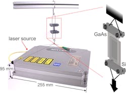
After this evidence, we extended the approach to gallium arsenide (GaAs). This not only shows the ability to weld other semiconductors but also to bond them in different multi-material configurations. The demonstrated performances in these other instances was also very high, with an average bonding strength of ~15 MPa for all tested cases (see Figs. 2 and 3). It shows the potential for laser welding of similar and dissimilar semiconductors, and then complex microsystem assembly configurations with a semiconductor as the top material.Interestingly, during our quest to successfully achieve semiconductor laser welding, we had to take a step backward and use nanosecond pulses, whereas the common trend in laser material processing is to use shorter and shorter pulses going into the femtosecond regime. Remarkably, all experiments were performed using a commercial, compact, and cost-effective fiber laser source. This indicates the possibility of scaling up the process to large wafers with the use of industrial high-power sources, and opens the door to easily integrate this approach into production lines of the industrial sector of microelectronics.
Joining complex architectures and multisemiconductor configurations
In comparison to alternative additive manufacturing technologies applicable to semiconductors (e.g., molecular wafer bonding), a unique advantage of our demonstrated laser solution is the possibility to join complex architectures and multisemiconductor configurations that would not be possible otherwise.
Since laser beams can be precisely guided, whole wafers or large pieces don’t need to be processed to be bonded. By selectively irradiating the desired area, small pieces with complex shapes can be easily welded with high precision.
This opens the door for new manufacturing practices in electronics, mid-IR photonics, and microelectromechanical systems (MEMS). Moreover, such flexible assembly process also holds potential for the emerging new concepts of hybrid chips as, for instance, co-designed electronics and microfluidics systems for sustainable cooling solutions in highly demanding semiconductor technologies.
REFERENCE
1. See www.univ-amu.fr/index.php/en/node/6563.
FURTHER READING
P. Sopeña et al., Laser Photonics Rev., 16, 2200208 (2022); https://doi.org/10.1002/lpor.202200208.
David Grojo | Research Director, Laboratoire LP3, Aix-Marseille University
Dr. David Grojo is research director of LP3, a joint laboratory between the French National Center for Scientific Research and Aix-Marseille University (Marseille, France).
Pol Sopeña | Postdoctoral Researcher, Laboratoire LP3, Aix-Marseille University
Pol Sopeña is a postdoctoral researcher at LP3, a joint laboratory between the French National Center for Scientific Research and Aix-Marseille University (Marseille, France).


