High-intensity, red LED developments may enable monolithic, RGB microLED devices
If scientists and engineers find a single material on which red, green, and blue (RGB) light-emitting diodes (LEDs) can be fabricated, it may help microLEDs become the dominant display technology. That’s because, while microLED performance is compelling, costs remain high.
By integrating the three primary colors on a single chip, the smaller LED emitters would reduce several major cost factors by requiring less device material, and reducing the cost of packaging LEDs, and then assembling them onto the module circuit boards. One challenge, however, is that all the LEDs must also fall within a certain range of luminance and wavelength to achieve the kind of performance demanded by end users.
Today, using various materials, electrical engineers design bright LEDs that produce light with wavelengths between ultraviolet and infrared, which includes the visible spectrum. Nitride semiconductors, a popular material compound under heavy development, are crystals containing nitrogen that, in theory, can produce monolithic RGB LEDs.
Traditional gallium nitride (GaN)-based blue and green LEDs are grown on sapphire epiwafers with a 2–6 in. substrate size. To lower costs, larger wafer sizes are desirable. Consequently, GaN-on-silicon epiwafers are also being used to grow green and blue microLEDs at 8 in. sizes now, with the potential to go to 12 in. wafers later. This is pushing the LED wafer makers to improve the way the LEDs are fabricated. New MOCVD chambers with much better uniformity and layer control are now available to enable most of the wafer to fall within quality control guidelines.
Likewise, indium gallium nitride (InGaN)-based blue and green LEDs have become increasingly prevalent in illumination and display applications, such as interior/exterior lighting and display backlights. However, their performance declines rapidly with the emission wavelength, especially in the red region. This decline is related to the content of indium in InGaN quantum wells (QWs). InGaN layers with a high indium content have a high density of defects and a strong quantum-confined Stark effect (QCSE).
Much effort has been devoted to improving InGaN-based red LEDs, with approaches including InGaN quantum dots, a semipolar InGaN buffer layer, lattice-matched InGaN/ScAlMgO4(0001) templates, and InGaN/GaN nanowires. However, up to now, engineers have struggled to make bright-red LEDs with this crystal.
While some groups have succeeded in making orange, pure red has been elusive. But for the first time, a team of electrical engineers at King Abdullah University of Science and Technology (KAUST; Thuwal, Saudi Arabia) have developed a crystal-growth system to realize high-intensity, low-voltage, pure-red LEDs using nitride semiconductors. The key to their success is replacing a larger portion of the gallium with the element indium to make InGaN-based red LEDs.
Overcoming challenges
The team’s high-temperature InGaN growth technique realized deep-red electroluminescence (EL) with 740 nm emission. Recently, a very-low forward voltage of 2.45 V at 20 mA was demonstrated in a 665 nm InGaN-based red LED on a β-Ga2O3 substrate. However, to succeed, the KAUST team had to overcome two key challenges.
First, because the indium easily evaporated from the crystal, they developed a novel, higher-pressure metalorganic vapor-phase epitaxy (MOVPE) reactor in which the InGaN-based red LED epitaxial wafers were grown on c-plane patterned sapphire substrates. Operating at 100 kPa, the single-wafer horizontal MOVPE reactor uses extra indium vapor above the crystal’s surface, achieving much better uniformity and layer control. The added pressure prevents the indium in the crystal from escaping and produces a higher indium concentration at the surface.
The second challenge was due to the fact that indium atoms are larger than gallium atoms, causing defects in the crystal to occur when they are introduced, degrading the quality of the light output. To overcome this, the team adds aluminum (Al), which has small atoms, that reduce the strain on the crystal, resulting in fewer crystal defects. In addition to the AlN/AlGaN barriers, other strain compensation approaches were proposed, such as hybrid QW structures and different thicknesses of GaN templates.1
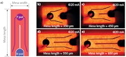
By designing rectangular chips with different mesa lengths (see Fig. 1), the team investigated the effects of size on electrical and optical properties of the InGaN-based red LEDs. Larger chips exhibited lower forward voltages because of their lower series resistances (see Fig. 2). A larger chip helped to realize a longer emission wavelength, narrower full-width at half-maximum, and higher external quantum efficiency.However, temperature-dependent electroluminescence measurements indicated that larger chips are detrimental to applications where high temperature tolerance is required. In contrast, a smaller red LED chip achieved a high characteristic temperature of 399 K and a small red-shift tendency of 0.066 nm K-1, thus showing potential for temperature-tolerant lighting applications.
REFERENCE
1. Z. Zhuang, D. Iida, and K. Ohkawaa, Appl. Phys. Lett., 116, 173501 (2020); https://doi.org/10.1063/5.0006910.

John Lewis | Editor in Chief (2018-2021)
John Lewis served as Editor in Chief of Laser Focus World from August 2018 through October 2021, after having served as the Editor in Chief of Vision Systems Design from 2016 to 2018. He has technical, industry, and journalistic qualifications, with more than 13 years of progressive content development experience working at Cognex Corporation. Prior to Cognex where his articles on machine vision were published in dozens of trade journals, he was a technical editor for Design News, covering automation, machine vision, and other engineering topics, for over six years.

