Researchers demonstrate first electrically injected GeSn laser

If materials science researchers and engineers have their way, they will develop monolithic lasers using silicon (Si), germanium (Ge), and tin (Sn)—which are all part of the same Group IV semiconductor family. The reason? Such a development could significantly improve microprocessing speed and efficiency, while reducing the size and cost of future on-chip photonics and nanoelectronics. That’s because GeSn epitaxy is fully compatible with complementary metal-oxide semiconductor (CMOS) processes, and GeSn, with Sn content over 8%, is a direct-bandgap material that enables efficient light emission over a broad wavelength range, making it versatile for midinfrared applications such as bio/chemical sensing, spectroscopy, and pyrometry.
In recent years, researchers have made significant progress in the development of optically pumped GeSn lasers, however, until last month, achieving electrically injected GeSn lasers has remained elusive. That’s when US-based materials science researchers, led by electrical engineering professor Shui-Qing ‘Fisher’ Yu, demonstrated what they claim to be the first electrically injected laser made with GeSn.1 The research was sponsored by the Air Force Office of Scientific Research.
Yu and Yiyin Zhou, a University of Arkansas (Fayetteville, AR) doctoral student in the microelectronics-photonics program, worked with colleagues at several institutions, including Arizona State University (Tempe, AZ), the University of Massachusetts Boston (Boston, MA), Dartmouth College (Hanover, NH), and Wilkes University (Wilkes-Barre, PA). The researchers also collaborated with semiconductor equipment manufacturer Arktonics (also in Fayetteville, AR).
Structure growth process
According to the paper, the laser-diode structure was grown using an industry-standard chemical vapor deposition (CVD) reactor with commercially available precursors on a 200 mm (100) Si substrate. Growing the GeSn/SiGeSn double heterostructure ensures carrier-and-optical confinement, according to the researchers, and the diode lasers were fabricated to address the hole leakage due to a type II band alignment between GeSn lasers. GeSn and the top SiGeSn barrier, the p-type top SiGeSn layer, was designed to facilitate the hole injection.
To this effect, five epitaxial layers were grown from bottom to top: first, a nominal 500-nm-thick strain relaxed Ge buffer layer, with n-type doping of 1 × 1019 cm3; next, a 700-nm-thick GeSn buffer layer using the spontaneous relaxation enhanced growth method, with nominal Sn composition from 8% (bottom) to 11% (top) and n-type doping of 1 × 1019 cm3; third, a nominally intrinsic 1000-nm-thick Ge0.89Sn0.11 active layer; fourth, a 170-nm Si0.03Ge0.89Sn0.08 cap layer with p-type doping of 1 × 1018 cm3; and finally, a 70 nm Si0.03Ge0.89Sn0.08 ohmic contact layer with p-type doping of 1 × 1019 cm3. All doping growth was done in situ by introducing corresponding doping gases. Researchers used x-ray diffraction and transmission electron microscopy techniques to measure the compositions of Sn and layer thickness.
After the sample growth, 80-μm-wide ridge-waveguide laser structures were fabricated via wet etching and then cleaved into individual devices with the cavity lengths of 0.3, 0.5, 0.8, and 1.7 mm. Etching depth was controlled at 1.4 μm to expose the GeSn buffer layer for metal contacts. Electron-beam-evaporated Cr and Au were deposited as both p and n electrodes through a liftoff process with thicknesses of 10 nm and 350 nm, respectively. The Si substrate was lapped down to 140 μm thick, followed by cleaving to form the Fabry-Perot cavity. Finally, the devices were wire-bonded to a Si chip carrier and mounted in a cryostat for low-temperature measurements.
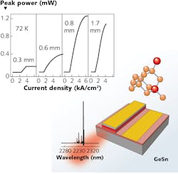
After fabricating the ridge waveguide GeSn laser, pulsed lasing was observed up to 100 K. The threshold was measured at 598 A/cm2 at 10 K. The characteristic temperature T0 was extracted from 76 to 99 K at the temperature range of 10 to 77 K for different devices. The threshold was measured at 598 A/cm2 at 10 K. The current-voltage (IV) measurement was performed using a direct-current source measurement unit. For the pulsed measurement, a pulsed high-compliance voltage source was used to drive the laser, and the current was monitored by a calibrated magnetically coupled current meter (see figure).
The electroluminescence and photoluminescence emission signal was collected and analyzed through a monochromator (10 nm resolution) and liquid-nitrogen-cooled InSb detector (response range 1 to 5.5 μm). The high-resolution spectra were obtained by using a Fourier transform infrared spectroscopy (FTIR) instrument equipped with the InSb detector. Step-scan mode was used with a 0.25 cm-1 resolution for the measurement.
Electrically injected lasers such as this GeSn laser are more challenging to achieve due to the need for doping and building structures. However, investigations of alternative structure designs are underway to further improve the device performance. Experiments include increasing the Sn content to boost the bandgap directness so that injection efficiency can be increased.
REFERENCE
1. Y. Zhou et al., Optica, 7, 8, 924–928 (2020); https://doi.org/10.1364/optica.395687.

John Lewis | Editor in Chief (2018-2021)
John Lewis served as Editor in Chief of Laser Focus World from August 2018 through October 2021, after having served as the Editor in Chief of Vision Systems Design from 2016 to 2018. He has technical, industry, and journalistic qualifications, with more than 13 years of progressive content development experience working at Cognex Corporation. Prior to Cognex where his articles on machine vision were published in dozens of trade journals, he was a technical editor for Design News, covering automation, machine vision, and other engineering topics, for over six years.