Scaled-up plasmonic receiver/emitter can boost free-space optical communications
With the advent and growth of the Internet of Things (IoT) in the factory and home, communications between myriad small smart devices are in need of a boost in speed. Because visible and near-infrared light have the potential to transmit information via free space at higher rates than radio-based WiFi, light-based wireless communications is now a hot topic. Researchers at Duke University (Durham, NC) and Facebook’s Connectivity Lab (Menlo Park, CA) have now placed their entry in this field by scaling up a previously miniature photonics technology—plasmonics combined with fluorescent materials—to a size and efficiency that shows potential for free-space optical communications (FSOC) that could not only supplant WiFi applications for IoT, but could replace some fiber-optic links as well.1
In 2016, researchers from the Connectivity Lab outlined a new type of light detector that could potentially be used for FSOC. Traditionally, hard-wired fiber-optic connections can be much faster than radio-wave wireless connections, but using light in wireless devices is more difficult. Current setups use either LEDs or lasers aimed at detectors that can reorient themselves to optimize the connection. It would be much more efficient, however, if a detector could capture light from different directions all at once. The catch is that increasing the size of an optical receiver also makes it slower.
This was also the case for the Connectivity Lab’s design. A spherical bundle of fluorescent fibers captured blue laser light from any direction and re-emitted green light that could be funneled onto a small receiver. While the prototype was able to achieve rates of 2 Gbit/s, most fiber-optic Internet providers offer up to 10 Gbit/s, and higher-end systems can push into the terabit-per-second (Tbit/s) region.
Looking for a way to speed up their FSOC designs, the Connectivity Lab turned to Maiken Mikkelsen, a professor at Duke University. Over the past decade, Mikkelsen has been a leading researcher in the field of plasmonics. “The Connectivity Lab’s prototype was constrained by the emissions lifetime of the fluorescent dye they were using, causing it to be inefficient and slow,” says Mikkelsen. “They wanted to increase the efficiency and came across my work showing ultrafast response times in fluorescent systems. My research had only proven that these efficiency rates were possible on single, nanoscale systems, so we didn’t know if it could scale up to a centimeter-scale detector.”
All previous work, Mikkelsen explains, has been proof-of-principle demonstrations with a single antenna. These systems typically involve metal nanocubes spaced tens to hundreds of nanometers apart and placed a few nanometers above a metal film. While an experiment might use tens of thousands of nanocubes over a large area, research showing its potential for superfast properties has historically cherry-picked just one cube for measurement.
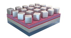
Plasmonic nanocubes
To scale up the device, Mikkelsen and Andrew Traverso, a postdoctoral researcher working in her laboratory, brought a more purposeful and optimized design to a large-area plasmonic device. Silver nanocubes 60 nm wide are spaced about 200 nm apart, covering 17% of the 1.2-cm-diameter device’s surface. These nanocubes sit 7 nm above a thin layer of silver, spaced by a coating of polymer that is packed with four layers of a photostable high-quantum-yield fluorescent dye.
The nanocubes interact with the silver base in a way that enhances the localized electromagnetic field, therefore enhancing the photonic capabilities of the fluorescent dye and causing a 910-fold increase in the overall fluorescence and a 133-fold emission rate enhancement. The superfast antenna also can capture light from a 120° field of view and convert it to a directional source with a record-high overall efficiency of 30%; the emission has a full width at half maximum (FWHM) angular spread of about ±35°.
Traverso notes that the fabrication method can be easily transferred to larger fabrication facilities. “We can create these large-scale plasmonic metasurfaces in under an hour with pipettes and Petri dishes, just simple liquid depositions on metal films,” he says.
The overall effect of the demonstration is the ability to capture light from a large field of view and funnel it into a narrow cone without losing any speed. To move forward with this technology, researchers would need to piece several plasmonic devices together to cover a 360° field of view and once again include a separate interior detector. While there is work to be done, the researchers see a viable path forward.
“In this demonstration, our structure acts to efficiently relay the photons from a wide angle into a narrow angle without losing speed,” says Mikkelsen. “We didn’t integrate a regular fast photodetector like the Connectivity Lab did in their original paper yet. But we solved the major bottleneck in the design and the future applications are very exciting.”
REFERENCE
1. A. J. Traverso et al., Optica (2021); https://doi.org/10.1364/optica.400731.

John Wallace | Senior Technical Editor (1998-2022)
John Wallace was with Laser Focus World for nearly 25 years, retiring in late June 2022. He obtained a bachelor's degree in mechanical engineering and physics at Rutgers University and a master's in optical engineering at the University of Rochester. Before becoming an editor, John worked as an engineer at RCA, Exxon, Eastman Kodak, and GCA Corporation.
