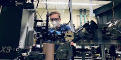
A team at Cornell University has developed a new, more powerful deep-UV laser using a new technique to grow semiconductor materials with pristine crystalline quality. And it’s already showing potential for various applications, including the sterilization of medical tools.
The new method—molecular beam homoepitaxy—enables the growth of crystalline wurtzite aluminum gallium nitride (AlGaN) films and heterostructures on aluminum nitride (AlN) crystals; crystal lattice matching enables growth of the purest quality materials with low point defect and dislocation densities, resulting in low optical loss. Len van Deurzen, an applied physics doctoral candidate at Cornell who led the research (working in part with Ryan Page, a materials science doctoral candidate), says the accurate growth of multiple AlGaN layers stacked on top of each other and the control over their interface quality and defect density was crucial (see Fig. 1).
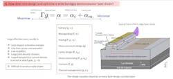
The team needed to create an optical cavity from the stacked layers to trap emitted light and promote stimulated emission (necessary for the laser). Once their material was available, the researchers, with help from Cornell’s NanoScale Science and Technology Facility, fabricated Fabry-Pérot-based micron-scale optical resonators on the AlN, a requirement for the deep-UV laser (see Fig. 2).Semiconductor lasers—namely those emitting in the deep-UV—generally also require pristine quality to support such requirements.
Another requirement is population inversion, which is the redistribution of atomic energy levels in a system that laser action happen; more specifically, it’s a phenomenon in which the electron quantum states mostly populate excited energy levels rather than the ground state and cause the material to produce optical gain. This was achieved using an optical pump.
Optical gain is also needed to optimize a laser, but this can be limited by short, free-carrier lifetimes due to defects. “Laser design also involves minimizing optical losses, where defects can scatter and absorb light—this is bad and can inhibit lasing,” van Deurzen says. “Lasing is only achieved once the optical gain equals the optical losses.” The improved, high-grade crystal quality created by the new molecular beam homoepitaxy technique is helping the Cornell team jump this hurdle.
Another hurdle in developing a deep-UV laser exists with the wide-bandgap semiconductor AlGaN’s natural material properties, such as effective masses that result in large dopant activation energies, low mobilities, large band edge density of states, and large transparency current density.
The Cornell team is not alone in battling these challenging material properties.
A team at Nagoya University in Japan used a different growth technique: metal-organic chemical vapor deposition (MOCVD) to develop deep-UV diode laser (published in Applied Physics Express in 2019). They achieved electrically pumped lasing with AlGaN high aluminum mole fraction—the ratio of the moles (a unit of measurement used to assess things like atoms and molecules) of Al to the total moles of all components present.
The UV-C (shortest-wavelength UV light) and UV-B (medium-wavelength UV light) laser diodes created by MOCVD use a material property of wurtzite aluminum gallium nitride: its pyroelectric nature, which is the result of the ratio of the wurtzite “a” (in-plane) and “c” (vertical) lattice parameters and the inversion asymmetry of the wurtzite crystal. This causes charge build-up at the interfaces of different AlGaN layers and electric fields inside the semiconductor, even when no voltage is applied.
According to van Deurzen, this effect can help overcome some of the existing ultrawide-bandgap laser challenges, particularly in a semiconductor’s high acceptor dopant activation energy and corresponding low hole concentration. The way this is used is by spatially grading the AlGaN crystal’s aluminum and gallium mole fraction along the inversion asymmetric direction. The resulting polarization charge can enhance the hole concentration.
The Cornell team’s molecular beam homoepitaxy could advance the usage of interface charges.
Polarization fields can aid the increase of electron and hole injection efficiency, a property of laser diodes—essentially, it determines what fraction of electrons and holes can be confined in the quantum wells. A low injection efficiency at high currents is currently a limiting factor in making deep-UV laser diodes useful and marketable, explains van Deurzen. Yet, molecular-beam epitaxy could provide the solution.
“We believe our molecular beam homoepitaxial growth technique has certain unique capabilities and device concepts,” he says. “It enables low chemical background impurities, the possibility of doping p-type layers that are not on the surface, the possibility of creating sharp doping profiles, and the possibility of growing monolayer-thick quantum wells. In short, these capabilities give more control over polarization fields and could potentially reduce the already low optical losses, but more importantly, allow for enhanced carrier transport and optical gain.”
What’s next?
“The versatility of AlN and GaN are well known, particularly in the electronics community,” van Deurzen says, citing applications in high-power and radio-frequency amplifiers used in 5G and developing 6G technologies.
The AlGaN material works for deep UV lasers and LEDs because of the direct bandgap of the wurtzite semiconductors, as well as the possibility of doping to achieve both n- and p-type conductivity. Such a range of uses “makes this material system a true goldmine of possibilities,” he says.
“UV-C light is great at sterilizing objects,” he says. “UV-C photons (~5 eV) have the right energy to break chemical bonds in bacteria and viruses, inactivating them. This is already done today with deep-UV LEDs or mercury vapor lamps. But where the former is fairly low in output power and does not inherently produce a directional emission pattern, the latter is generally inefficient, bulky, and can be a health hazard. A laser diode is also unique in having the advantage of producing directional, efficient, coherent, and high-intensity light output.”
Semiconductor-based laser diodes, such as the deep-UV laser more effectively created with the Cornell team’s material growth technique, are small (with chips a few cubic millimeters in size) and more efficient. They also sport long lifetimes, have the potential for pulsed- and continuous-wave mode capabilities, and are tunable in wavelength by changing the Al and Ga mole fractions in AlGaN.
van Deurzen also sees potential for commercialized deep-UV lasers in advanced gas sensing, water purification, quantum metrology and spectroscopy, and precision photolithography.
“And there will certainly be applications that we do not yet anticipate,” he says, citing the versatility of his team’s new semiconductor material growth method in improving the use of UV light. “There is something unknown and exciting around the corner.”
REFERENCE
1. Z. Zhang et al., Appl. Phys. Express, 12, 124003 (2019); https://doi.org/10.7567/1882-0786/ab50e0.

Justine Murphy | Multimedia Director, Digital Infrastructure
Justine Murphy is the multimedia director for Endeavor Business Media's Digital Infrastructure Group. She is a multiple award-winning writer and editor with more 20 years of experience in newspaper publishing as well as public relations, marketing, and communications. For nearly 10 years, she has covered all facets of the optics and photonics industry as an editor, writer, web news anchor, and podcast host for an internationally reaching magazine publishing company. Her work has earned accolades from the New England Press Association as well as the SIIA/Jesse H. Neal Awards. She received a B.A. from the Massachusetts College of Liberal Arts.

