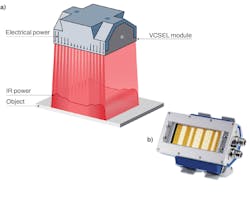
High-power vertical-cavity surface-emitting laser (VCSEL) heating systems are a unique manufacturing tool for various processes, including welding, joining, softening, drying, and soldering. These systems can heat large surfaces with directed infrared (IR) radiation, operating at the 980 nm wavelength—a perfect match for most heating processes and application fields.
VCSEL systems consist of many single emitters, each containing about 125,000 individual VCSELs in two separate zones. A unique feature of this setup is that the irradiation can be controlled in a highly accurate way, because the IR emission of the system can be set independently per zone. TRUMPF’s standard VCSEL system, for example, can be customized and scaled from 2.4 to 19.2 kW to reach the required output power.
Individual heating profiles can be created along the system-axis to guarantee heat is only applied to the target material where needed (see Fig. 1). This setup enables homogenous heat treatment of large target areas. VCSEL systems also tout high process speeds, as the standard irradiance is more than 100 W/cm2—which can be increased to 400 W/cm2 by adding a collimating lens to the system. Regarding the materials to be processed, robust VCSEL systems offer high tolerance to back reflections. And within the process chain, VCSEL systems are easy to integrate because they are compact and have an even smaller footprint compared to other solutions such as reflow ovens.
More efficiency in microchip assembly
The electronics industry is facing an ever-increasing demand for microchips. At the same time, industries including consumer electronics request miniaturization of integrated components, as devices become lighter, thinner, and smaller. The industry is replacing bonding processes with flip-chip assemblies. Also, design engineers are facing the challenge of realizing flatter designs of microelectronics assemblies. Smart devices such as mobile wearables are one example of this—they demand more functionalities within smaller devices. Consequently, the trend in microchip manufacturing goes toward smaller dies and the demand for time reduction and more efficiency.
VCSEL heating systems, such as those developed by TRUMPF, for laser-assisted soldering (LAS) and laser-assisted bonding (LAB) processes address the need of the electronics industry for a more efficient flip-chip assembly. Using direct heat treatment via VCSEL high-power systems, die attach and assembly processes can be sped up and the quality of solder interfaces increased. Interfacial intermetallic compound growth in the solder interface is virtually inhibited, due to the short process time.
VCSEL systems already have a rectangular emitting area, leading to a rectangular laser beam profile. Therefore, no additional optics are needed for these applications. By using VCSEL heating systems for LAS and LAB, cycle times can be reduced by up to an order of magnitude compared to standard reflow soldering processes.
The quality and reliability of PCB assemblies are increasing as VCSEL heating systems work with high precision and the heat is only applied on the PCB and semiconductor die where it’s needed. This results in a more energy-efficient process, and the quality and lifetime of the die attach as well as of the assemblies are increasing. So, solder interfaces benefit from the VCSEL-based technology.
Microstructure analyses confirm up to 3X less warpage when using a VCSEL heating system to solder interfaces. The assembly process also benefits from very repeatable and accurate die soldering and bonding conditions, because the VCSEL heating system allows homogenous illumination, fast switching times, and precise power control. Another aspect is the overall footprint for microchip assembly. It can be reduced compared to conventional reflow solutions because the VCSEL heating systems are very compact; in the case of LAB, for example, the footprint can be reduced by up to 30%. Reflow soldering remains the status quo in microchip assembly, but VCSEL heating systems will be a sustainable alternative process method that leads to overall increase in efficiency.LAS, LAB, and how they work
LAS is the process in which solder balls are soldered directly onto the PCB using VCSEL IR heat treatment (see Fig. 2a). This supports the trend toward using smaller solder balls and pitches, which also allows for a reduction in the overall building space needed in consumer electronics. During the LAB process, a flip chip is placed onto a PCB board, using solder balls as a connection. The VCSEL system heats the chip from above, and laser energy is transmitted through the chip to melt the solder balls between the chip and PCB (see Fig. 2b). VCSEL heating systems can be used for stationary heating or for continuous heating processes. VCSEL-based systems offer large, controllable heating areas with higher power compared to other solutions.
Ronald Verstraeten | Application Engineering Manager for Industrial Heating, TRUMPF Photonic Components
Ronald Verstraeten is the application engineering manager for industrial heating at TRUMPF Photonic Components (Ulm, Germany).

