High-performance chip-scale lasers have arrived
At long last, a key missing component to achieve complete miniaturization via integrated photonics is here: High-performance chip-scale lasers.
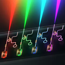
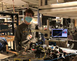
Michal Lipson’s Nanophotonics Group at Columbia (see Fig. 1) recently demonstrated a high-performance visible-light laser platform that fits on a fingertip (see video). Their chip-scale lasers are the first platform to enable tunable and narrow linewidth chip-scale lasers for wavelengths shorter than red, with the smallest footprint and shortest wavelength (404 nm).
The group’s platform offers performance metrics such as tuning range, tuning speed, linewidth, power, and side mode suppression ratio (SMSR) previously only achieved in benchtop and expensive laser systems—opening the door to applications in quantum optics, atomic clocks, biosensing, laser displays for augmented reality (AR)/virtual reality (VR), and underwater Li-Fi.
“When working on integrated photonics with visible light, we realized high-performance visible lasers are bulky and expensive, which makes it difficult for most research labs to have access to them,” says Mateus Corato-Zanarella, an electrical engineering Ph.D. student who helped create the platform.
Several important applications such as portable atomic clocks and AR/VR technologies “can’t afford benchtop lasers to power their optical systems,” he says. “The need for compact, inexpensive, high-performance visible lasers was apparent, so we decided to use integrated photonics to make them.”
Creating a chip-scale laser platform
The most important concept behind the group’s chip-scale laser platform (see Fig. 2) is self-injection locking, which is the process of modifying the emission of a laser by reflecting a portion of its output light back to the laser cavity.
“In our work, we used our designed photonic integrated circuit (PIC) to modify and control the emission of existing laser diodes using this physical phenomenon,” explains Corato-Zanarella. “Each laser originally emits light of multiple wavelengths that are shades of a given color. Using a low-loss microring resonator-based feedback loop in our PIC, we select a single wavelength and reflect a portion of its light back to the diode.”
This selective optical feedback makes the chosen lasing mode “win the competition for gain over all others, collapsing all the optical power of the laser to it and resulting in a single-frequency emission of narrow linewidth,” Corato-Zanarella says. “By electrically controlling the microring resonator via on-chip phase shifters, we choose which lasing mode wins and consequently tune the wavelength of the emitted light.”
This self-injection locking concept has been used over the years in external, often bulky, cavity lasers, “and now we’re applying it to a photonic integrated platform designed for visible wavelengths,” he adds.
Applications galore
The most surprising aspect of the group’s work is how powerful their integrated laser platform is, enabling lasers with state-of-the-art metrics in a chip-scale form factor. “Our work breaks the paradigm that high-performance visible lasers need to be benchtop—opening the door to fully integrated visible light systems for numerous applications,” says Corato-Zanarella.
For starters, it can be used for quantum information because most quantum bits for quantum computation trap or probe atoms or ions via visible light. “The light must be very pure (narrow linewidth) and have very specific wavelengths to address atomic transitions,” Corato-Zanarella notes. “Currently, lasers available for these applications are expensive and benchtop. These bulky sources can be replaced by tiny and inexpensive chips, which will enable quantum systems to be scaled down and eventually become part of the technologies accessible by the general public.”
Atomic clocks are also poised to benefit. “State-of-the-art atomic clocks are incredibly precise and based on strontium atoms, which must be trapped and probed by lasers of many different colors at the same time,” he says. “Similar to quantum optics systems, the massive size of currently available lasers confine this technology to research labs. Chip-scale lasers will make it possible to shrink these systems, with the goal of making portable atomic clocks.”
In biosensing, several neural probes use optogenetics to measure, modify, and understand neural responses. “In optogenetics, neurons are genetically modified to produce a type of protein, opsins, which are sensitive to visible light,” says Corato-Zanarella. “By shining visible light, typically blue, into these cells, scientists can turn on specific neurons at will. Similarly, in fluorescent imaging, fluorophores need to excited with visible light to generate the desired images. Our high-performance compact lasers open the door to miniaturizing these systems.”
How about underwater ranging? “Underwater ranging requires blue or green light because ocean water strongly absorbs light of all other colors,” he says. “For the popular ranging strategy of frequency-modulated continuous-wave LiDAR, the laser needs to be speedily tunable for accurate sensing of the distance and velocity of objects. Our lasers could be used for portable underwater ranging systems using this technology.”
And then there’s Li-Fi. “As demand for bandwidth in communication systems increases, networks have become saturated,” says Corato-Zanarella. “Li-Fi, or visible light communications, promises to supplement traditional microwave links at the user end to overcome this bottleneck. And the high modulation speeds of our lasers are ideal for enabling extremely fast optical communication links.”
Challenges to get to chip-scale lasers
The biggest challenge for the group to overcome was how to simultaneously mitigate the high losses characteristic of integrated platforms at visible wavelengths and achieve robust broadband operation covering almost an octave.
“At wavelengths shorter than red, the coupling and propagation losses of photonic integrated circuits increase significantly, which has prevented the realization of high-performance lasers at these colors,” says Corato-Zanarella. “We solved the coupling loss problem by choosing Fabry-Perot (FP) diodes as the light sources, which minimizes the impact of the losses on the performance of the chip-scale lasers.”
Unlike other strategies that use different types of sources, the group’s approach enables the realization of lasers at record-short wavelengths (404 nm)—while also providing scalability to high optical powers.
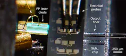
“FP laser diodes are inexpensive and compact solid-state lasers are widely used in research and industry, but they emit light of several wavelengths simultaneously and aren’t easily tunable, which prevents them from being used directly for applications requiring pure and precise lasers,” he explains. “By combining them with the specially designed photonic chip (see Fig. 3), we’re able to modify the laser emission to be single-frequency, narrow linewidth, and widely tunable.”
They overcame the propagation loss issue by designing their platform to minimize both the material absorption and surface scattering losses simultaneously for all the visible wavelengths. To guide the light, they used silicon nitride, a dielectric widely used by the semiconductor industry, which is transparent for visible light of all colors.
“Although there is minimal absorption, the light still experiences loss due to unavoidable roughness from the fabrication processes,” Corato-Zanarella says. “We solved this problem by designing a photonic circuit with a special type of ring resonator. The ring has a variable width along its circumference, allowing for single-mode operation characteristic of narrow waveguides and low loss characteristic of wide waveguides.”
The resulting photonic circuit provides a wavelength-selective optical feedback to the FP diodes that forces the laser to emit at a single desired wavelength at very narrow linewidth.
By combining these intricately designed pieces, the group built a robust and versatile platform that’s scalable and works for all colors of light.
Patent pending
The group has filed a patent for their technology, and their next steps “involve working on the optical and electrical packaging of our chip-scale lasers to turn them into standalone units, which we can then easily use in applications such as quantum optics, imaging, and sensing,” says Corato-Zanarella.
FURTHER READING
M. Corato-Zanarella et al., Nat. Photon., 17, 157–164 (2023); https://doi.org/10.1038/s41566-022-01120-w.
About the Author
Sally Cole Johnson
Editor in Chief
Sally Cole Johnson, Laser Focus World’s editor in chief, is a science and technology journalist who specializes in physics and semiconductors.


