SEMICONDUCTOR LASERS: Optically pumped semiconductor lasers expand the scope of potential applications
The optically pumped semiconductor (OPS) laser has gained significant market share in recent years for low-power applications, primarily in OEM bioinstrumentation applications at the 488 nm heritage wavelength, as well as 473 nm for photofinishing. Optically pumped semiconductor lasers have succeeded in these applications because they offer major advantages over earlier laser types while avoiding many of their limitations. Now the wavelength and power scalability of this technology are beginning to be more fully exploited, resulting in new wavelengths and high output powers that are leading OPS lasers into a much wider applications space.
Most semiconductor lasers are constructed as so-called edge emitters. Here, the light is emitted in the plane of the active junction from an area measuring a few microns across, resulting in a highly divergent output beam. In addition, the output from most laser diodes is asymmetric and astigmatic. These characteristics led to the use of vertical-cavity semiconductor lasers (VCSELs) in certain telecom applications.
In a VCSEL, the light is emitted perpendicular to the junction and out the face of the diode chip. The larger output aperture results in a lower divergence beam that can also be symmetric. Unfortunately, electrically pumped VCSELs cannot produce the high power of an edge emitter, because there’s no way to flood a large area with charge carriers without using extended electrodes that would introduce too much loss. However, this problem can be avoided by optically pumping the device to create the charge carriers.
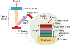
In an OPS laser, pump light from a direct-coupled single emitter or fiber-coupled laser-diode array is re-imaged into the front surface of the OPS chip (see Fig. 1). This monolithic III-V semiconductor chip contains layers of tertiary indium gallium arsenide (InGaAs) quantum wells alternated between binary gallium arsenide (GaAs) layers. The binary layers are optimized to efficiently absorb pump radiation, resulting in a high population of charge carriers. This leads to population inversion and recombination in the quantum wells, which emit at a wavelength determined by the stoichiometry and physical dimensions of the quantum-well structures. Behind these absorption/emission layers are several alternating high-index and low-index layers that act as a low-loss distributed-Bragg-reflector (DBR) mirror optimized for the specific OPS output wavelength.
Why not just integrate the semiconductor pump laser and VCSEL architecture on a single chip? First, external optics enable the laser cavity, and hence output-beam characteristics, to be tailored at will. Also, allowing access to the intracavity beam facilitates efficient and simple doubling of the near-IR output to produce a visible wavelength. In addition, it enables a high degree of power scaling because multiple pump diodes can be coupled into a single OPS chip.
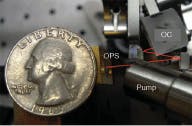
The pump radiation enters the OPS chip at an angle near 30°. This noncollinear approach fills the mode volume and introduces very little pump ellipticity while ensuring that the OPS intracavity beam is not clipped by the pump relay optic. In addition, this off-axis pump geometry allows two or even three pumps to be arranged azimuthally for high power generation. Just as important, the entire OPS pump head can be scaled and mounted on a small block, delivering a size advantage for OEM applications, as well as excellent short-term and long-term stability (see Fig. 2).
Wavelength and output mode
The OPS gain medium offers the designer several advantages over laser crystals, such as Nd:YAG and Nd:YVO4 (vanadate). For example, OPS lasers can operate over a very broad pump wavelength range. All that is required is that the pump-diode wavelength exceeds the bandgap for the OPS absorption layers. In contrast, Nd- and ytterbium (Yb)-doped materials have very sharp absorption peaks that must be precisely matched by the pump-diode wavelength, which requires careful diode selection (thereby reducing the yield) and tight control over diode operating temperature.
Another OPS advantage is the lack of thermal lensing, which can be quite strong in standard diode-pumped solid-state (DPSS) materials like Nd:YVO4. Moreover, the lensing effect scales with pump power, often significantly complicating cavity optimization and compromising power-scaling efforts.
From an end-user viewpoint, however, the most important benefit of OPS technology is the ability to readily customize it over a wide range of output wavelengths. For example, an indium gallium arsenide (InGaAs)-based OPS laser can produce output from 700 to 1200 nm. Frequency doubling extends this operation through most of the visible spectrum (350 to 600 nm). This wide range enables OPS lasers to be designed to fit the application instead of vice versa.
Another significant OPS advantage is its longitudinal-mode characteristics, which result in low noise in the frequency-doubled output. Intracavity-doubled continuous-wave (CW) lasers often suffer from mode noise because power oscillates dynamically between different longitudinal modes. Because second-harmonic-generation (SHG) efficiency depends on the precise wavelength of the fundamental, this mode noise translates into amplitude noise in the doubled output (often called “green noise”). In commercial OPS lasers, a narrowband birefringent filter (BRF) is used to narrow the output and hold its wavelength at the peak of the SHG curve. This birefringent filter limits the output to between three and ten stable longitudinal modes. Moreover, the very short excited-state lifetime for the OPS quantum wells virtually eliminates dynamic power oscillation between these modes, resulting in green noise of less than 0.03% (up to 10 MHz rms). In addition, the wide mode spacing in the short OPS cavity makes it relatively easy to incorporate an intracavity etalon to force the laser to oscillate at a single longitudinal mode for high-coherence applications.
Power scaling
The power from an OPS laser can be increased by using more-powerful pump diodes or by increasing the number of pump diodes. However, the lasing efficiency (L-I slope or optical output versus input current) of an OPS laser (or any other VCSEL) rolls off at higher power and, ultimately, even goes negative. This is all due to thermal effects and the physics of population inversions. Simply stated, as the density of carriers and the photon flux is increased, the temperature in the quantum wells rises. Coherent engineers have developed a two-pronged approach to circumvent this issue and enable OPS power scaling.
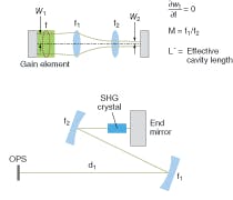
The first innovation is to use an expanded mode volume and a novel folded-cavity design. Because power density is responsible for the temperature increase, an obvious solution is to spread the power over a wider area of the OPS chip. But simply increasing the mode volume without increasing cavity focal length pushes the laser into an unstable operating regime comprising multiple transverse modes. On the other hand, dramatically increasing the cavity focal length would make the laser unnecessarily large and reduce optomechanical stability.
Instead, we use a compact, folded cavity incorporating Keplerian telescopic optics to uncouple mode diameter and cavity length. This arrangement simultaneously supports a large beam diameter in the OPS chip but with a narrow, well-behaved waist near the output mirror (see Fig. 3). Moreover, the SHG crystal can be located at this beam. Together with the low mode noise, this enables very efficient frequency doubling using a robust long-lived lithium triborate (LBO) crystal rather than an exotic crystal or waveguide, which is necessary to directly double some laser diodes.
We have also implemented an aggressive cooling scheme to directly lower the temperature in the OPS chip in general and within the quantum wells in particular. This cooling scheme is based on a new proprietary mounting technique for the chip on its heatsink. It allows higher power to be extracted from a given device size and is also one of the key factors responsible for the long lifetime of OPS lasers.
Current life-test data for 488 nm commercial products exceeds 50,000 hours for 20 mW models and more than 25,000 hours for 200 mW versions, strongly validating this approach. A 5 W, 532 nm laser is already in production, and 11.5 W of TEM00 output at 531 nm and nearly 20 W at 488 nm have both been demonstrated in the lab. Furthermore, these lasers are all highly compact.
Diverse applications
The first area to benefit from OPS technology was bioinstrumentation, initially at 488 nm. In fact, these lasers are now the dominant solid-state technology at 488 nm for applications such as confocal microscopy, flow cytometry, DNA sequencing and proteomics-applications that formerly utilized power-hungry ion lasers to excite fluorophores. The use of miniaturized OPS lasers has enabled simpler, smaller instruments with greater reliability, higher performance and lower power consumption. In addition, “wavelength on demand” OPS technology has recently delivered 505 nm lasers that can simultaneously excite a wide set of fluorophores that formerly required both 488 and 514 nm.
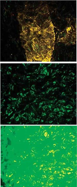
Trace-evidence recovery applications have also adopted OPS technology. Here, green lasers are used to reveal latent fingerprints and bodily fluids at crime scenes (see Fig. 4). Traditionally ion lasers were only practical for lab work, and even DPSS lasers were too bulky (and too costly) for this application. Now, the development of compact forensic imaging systems based on 5 W OPS lasers at 530 nm has enabled true field portability and affordability.
Medical (therapeutic) applications are also beginning to take advantage of OPS lasers. For example, a new 6 W yellow laser (at 577 nm) has been developed for photocoagulation ophthalmic treatments-sealing burst vessels at the back of the eye. Its yellow wavelength is considered ideal for this work because it matches the absorption maximum of blood. This wavelength and power level is also useful for some applications in dermatology.
In the area of displays, multiwatt OPS lasers at 460 and 530 nm are now widely used for digital film writing-creating a master film-in the movie industry, where scenes increasingly incorporate computer-generated effects. Moreover, similar lasers have been developed and demonstrated in prototypes of high-end RGB projection display applications (see www.laserfocusworld.com/articles/277186).
Matthias Schulze | Director of Marketing, OEM Components and Instrumentation at Coherent
Matthias Schulze is Director of Marketing, OEM Components and Instrumentation at Coherent (Santa Clara, CA).
Andrew Masters | Director of Marketing, Coherent
Andrew Masters is Director of Marketing at Coherent (Santa Clara, CA).


