PHOTONIC-CRYSTAL LASERS: Photonic crystals boost single-mode power in VCSELs
The addition of photonic-crystal structures to long-wavelength vertical-cavity surface-emitting lasers can increase single-mode output power to more than 3 mW, and could lead to more than 10 mW levels at shorter wavelengths.
DAN BIRKEDAL AND DIRK JESSEN
Vertical-cavity surface-emitting lasers (VCSELs) are popular because of their low power consumption, easy packaging, and easy fiber coupling based on their circular beam profile. Further, VCSELs are easily configured in laser arrays and allow for cost-efficient manufacturing.
Because oxide-confined VCSELs are limited in single-mode output power they have had the most commercial success in applications in which multimode operation is sufficient or in applications with limited single-mode power requirements-typically less than 1 mW. As a result, VCSEL lasers have become the first choice in short-range data-communications transmission and in consumer applications such as optical mice.
In longer-range and higher-speed datacom and telecom applications, edge-emitting Fabry-Perot and distributed-feedback lasers are used. However, Fabry-Perot lasers are limited in range by modal dispersion at higher modulation frequencies and distributed-feedback lasers often require the addition of an expensive optical isolator. Laser development has therefore recently focused on developing long-wavelength VCSEL lasers with sufficient single-mode power to address the increasing demand for cost-efficient telecom access-network solutions.
Long-wavelength VCSELs
A year ago Alight Technologies took over the dilute-nitride 1300 nm VCSEL technology platform from Infineon Technologies (Munich, Germany). Alight is now applying its proprietary photonic-crystal technology to increase single-mode output power at 1300 nm to meet the requirements of telecom access networks and to address a range of other communications applications. This photonic-crystal approach to dilute-nitride 1300 nm VCSELs is generic and can be applied to increase the single-mode output power of VCSELs at other wavelengths.
Conventional oxide-confined VCSELs
Commercially available 850 nm oxide-confined VCSELs are usually limited in single-mode output power to between 1 and 2 mW. The main reason for this limitation is that the oxide aperture confines the electrical current and the optical modes. To ensure operation in the fundamental mode, the oxide aperture has to be quite small (typically 3 to 4 µm for 850 nm VCSELs), which limits the amount of achievable output power. The small oxide aperture also results in a large differential resistance, which in turn leads to enhanced ohmic heating and difficulties in achieving high-speed operation. In addition, the small aperture typically degrades the lifetime and reliability of the VCSEL.
Enter photonic crystals
A promising approach for high-speed and high-power single-mode VCSELs is to use photonic crystals for lateral optical confinement in combination with oxide apertures for current confinement.1 The lateral-mode confinement by the photonic crystals can be implemented by etching a pattern of holes in the VCSEL top mirror, resulting in a cavity resonance-wavelength shift that corresponds to a change in the effective index.2 The cavity resonance-wavelength shift is very small for shallow etch depths of a few hundred nanometers in a VCSEL top mirror. Therefore, photonic-crystal VCSELs have been demonstrated by etching deep holes (10 to 20 mirror periods).3, 4, 5 The deep holes etched into the top mirror result in the intended shift in the cavity resonance wavelength and also in increased optical losses (reduced photon lifetime). In this case, both the photon lifetime and the cavity resonance-wavelength shift will determine the lateral-mode confinement. Unfortunately, this has so far resulted in strongly index- or loss-guided VCSELs with small mode areas and low optical output power.
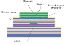
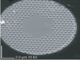
To combat these negative effects, Alight Technologies uses a different approach to photonic-crystal VCSELs. Shallow etches in a layer close to the active layers are followed by a deposition of a dielectric top mirror. The result is an enhanced tuning range for the cavity resonance, in which wavelength shifts of more than 10 nm for etch depths of only a few tens of nanometers have been demonstrated.6 Though early work confirmed this approach at 850 nm, this photonic-crystal technology is now being transferred to long-wavelength dilute-nitride VCSELs (see Fig. 1). A shallow etch in the semiconductor top surface defines a tridiagonal lattice of rods with a longer cavity resonance wavelength to implement the photonic-crystal structure. A photonic-crystal lasing defect is created by leaving out several rods in the center of the tridiagonal lattice (see Fig. 2).
FIGURE 2. An electron-beam micrograph reveals a photonic-crystal lasing defect for long-wavelength VCSELs that is created by leaving out several rods in the center of the tridiagonal lattice.
The use of a dielectric top mirror continues Infineon’s approach, which resulted in a qualified device with excellent reliability.7 The dielectric top mirror also reduces the optical losses due to free-carrier absorption as compared to a conventional semiconductor top mirror.
Results
Initial development and proof-of-concept work was done using 850 nm VCSEL materials technology. Although the development work was not completed because of a customer-driven refocus on the long-wavelength VCSEL work, single-mode operation of the photonic-crystal VCSELs with 8-µm-diameter mode sizes at 850 nm was achieved. Although single-mode power levels were limited to between 3 and 5 mW from ohmic heating because of nonoptimized contact processes, the development work indicated the possibility of achieving single-mode power levels on the order of 10 mW at 850 nm.
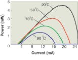
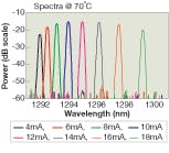
The free-carrier absorption is stronger at longer wavelengths, so development of long-wavelength VCSELs is inherently more difficult. Nonetheless, excellent initial results have been achieved by adapting the long-wavelength photonic-crystal designs to the epitaxial platform already developed by Infineon. For example, light-current characteristics show that devices are single-mode up to approximately 3 mW at 20°C and deliver 1.4 mW single-mode power at 90°C (see Fig. 3). The devices have excellent side-mode suppression ratios of greater than 30 dB for the entire current range at 70°C.
The use of photonic crystals allows precise engineering of the near field-to ensure excellent fiber-coupling characteristics-while maintaining single-mode operation (see Fig. 4). The far field of the long-wavelength VCSEL at 15 mA is nearly Gaussian and has a 1/e2 width of less than 17° over the operating-current range due to the large mode sizes possible using photonic crystals. Better than 80% coupling efficiencies to single-mode fibers have been achieved using standard bulk optics.
FIGURE 4. Far-field analysis at 1300 nm for the photonic-crystal VCSELs shows a nearly Gaussian shape with a 1/e2 width of less than 17º over the range of operating current.
The proximity of the photonic-crystal layer to the lasing cavity offers additional advantages. In particular, the number of mirror pairs remains constant over the entire structure, which is essential. In contrast to deeply etched structures, the total mirror reflectivity is unmodulated and remains at a high value. This characteristic results in structures in which the lateral guiding mechanisms are solely determined by the locally varying wavelength, or effective index, and not loss/gain guiding. Loss guiding would inevitably lead to additional internal optical losses (highly undesirable in high-power applications) and would distort the mode due to the strong confinement, leading to non-Gaussian far fields.
The weak guiding of the photonic crystal results in larger mode areas that allow for increased current (oxide) apertures, leading to benefits such as increased power and better reliability. The photonic-crystal structuring also enables polarization control, narrow beam divergence, and some wavelength tuning. And, because of the generic nature of the photonic-crystal approach, the designs can be scaled to suit a desired lasing wavelength, although constraints from lithography and reasonable mode and current aperture sizes limit the practical wavelength range to between 400 and 3000 nm.
1300 nm product focus
With time to market being essential, Alight has adopted a foundry approach based on manufacturing equipment acquired from Infineon. Close cooperation with a lead customer is also helping to decrease the time from prototyping to a qualified 1300 nm product. Because the generic photonic-crystal platform can be applied to many wavelengths and applications-including optical sensing, printing, passive optical fiber, and consumer electronics-the pursuit of opportunities outside the telecom and datacom markets through partnerships should help achieve maximum penetration of this proprietary photonic-crystal technology.
REFERENCES
1. S. Bischoff et al., Proc. European Conf. on Optical Communications (ECOC) 40 (2003).
2. G.R. Hadley, Optics Lett. 20(13) 1483 (1995).
3. H. Unold et al., Proc. ECOC 520 (2001).
4. J.J. Song et al., Applied Phys. Lett. 80(21) 3901 (2002).
5. T. Furukawa et al., Applied Phys. Lett. 85(22) 5161 (2004).
6. F.P. Romstad et al., Proc. ECOC 596 (2004).
7. G. Steinle et al., Proc. Electronic Components and Tech. Conf. (ECTC) 218 (2001).
DAN BIRKEDAL is CTO and founder and DIRK JESSEN is vice president of business development for Alight Technologies, Ryttermarken 15-21, DK-3520 Farum, Denmark; e-mail: [email protected]; www.alight.dk.


