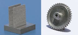
Femtosecond lasers combine additive and subtractive manufacturing
Most 3D printing or laser additive manufacturing (AM) systems use continuous-wave (CW) lasers. However, researchers at PolarOnyx (San Jose, CA) are pioneering AM instruments that use femtosecond pulsed lasers to create 3D objects from high-temperature materials. Furthermore, the well-known athermal ablation properties of ultrafast lasers can simultaneously accomplish subtractive manufacturing in one computer-controlled scanning process for combined additive/subtractive manufacturing that doubles the system's capability and increases productivity without adding cost.
By taking advantage of instantaneous high-temperature plasma generation, femtosecond fiber lasers can sinter such high-temperature metals as tungsten, with a melting temperature of 3422°C and thermal conductivity of 173 W/(m·K), and ceramics including zirconium diboride (ZrB2) with a melting temperature of 3246°C. By tuning the pulse width and energy, microstructure shape and size can be manipulated such that the melted structure is more robust against mechanical and thermal stresses than conventional CW laser AM. Tungsten gears and thin-walled (100 μm) components, for example, have been fabricated with femtosecond laser AM. Reference: S. Bai et al., Appl. Phys. A, 122, 5, 495 (May 2016).

Gail Overton | Senior Editor (2004-2020)
Gail has more than 30 years of engineering, marketing, product management, and editorial experience in the photonics and optical communications industry. Before joining the staff at Laser Focus World in 2004, she held many product management and product marketing roles in the fiber-optics industry, most notably at Hughes (El Segundo, CA), GTE Labs (Waltham, MA), Corning (Corning, NY), Photon Kinetics (Beaverton, OR), and Newport Corporation (Irvine, CA). During her marketing career, Gail published articles in WDM Solutions and Sensors magazine and traveled internationally to conduct product and sales training. Gail received her BS degree in physics, with an emphasis in optics, from San Diego State University in San Diego, CA in May 1986.
