GORAN PANDZA and YI CHENG
Since the introduction of commercial light-emitting diodes (LEDs) in the late 1960s, there has been a gradual adoption of the technology in a wide range of applications, from consumer products to public illumination, including specialized niches like machine vision for industrial devices or precise illumination in medical instrumentation. The technology has evolved substantially in the last few decades, and LEDs are now regarded as the best solution for illumination in most areas, providing high optical power with superior efficiency and low mass-production cost.
In a few market segments, current LED properties are less than satisfactory. These segments demand not only high-efficiency illumination, but also a high-quality radiation pattern from the LED. To meet these demands, iC-Haus has developed masked point-source LED technology. To illustrate the advantage of this technology, we compare masked point-source LED technology with current LED technology, and provide examples of where it can benefit an application.
Advancing LED design
LED technology is based on the principle of electro-luminescence; that is, the nonthermal conversion of electrical energy into light radiation (as opposed to incandescence, where the light radiation is generated through the emission of heat). LED operation relies on a simple semiconductor p-n junction, where positive and negative charge carriers recombine and release a photon. Selection of semiconductor material for the diode structure enables the wavelength of the emitted photon to be controlled, therefore enabling the device to produce visible, infrared (IR), or ultraviolet (UV) light.
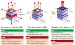
In a standard LED, light is emitted from the active area in all directions, the result of a process known as volumetric emission. In contrast, surface emission LEDs confine the active area within a section of the diode and emit light only from the top. In a further refinement, the manufacturing process can incorporate a reflective layer under the active area, thus redirecting the bottom illumination to the top surface and increasing the LED intensity and efficiency.
While the surface emission LED has an improved radiation pattern because light is emitted in only one direction, this is not always adequate. Some applications require extremely well-defined illumination patterns, which has led to the development of the masked point-source LED.
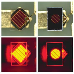
The masked point-source LED is based on the surface emission LED, but with some additional modifications. Above the n-doped semiconductor layer (cathode), a flat glass with reticle structures is added. This optical assembly defines the light emission aperture. Another important improvement to this design is that the bonding wire and contact are shifted to the edge of the semiconductor surface, removing it from the radiation path (see Fig. 1).
As a result, most properties of the surface emission LED are preserved, while concentrating the light emission in a specified aperture shape and size. At the same time, this design creates a clear path for uniform, well-defined illumination.
To summarize, the basic LED illumination properties are common to all design approaches and include high-efficiency light generation, long lifetime, low heat dissipation, selectable wavelength according to material, small size, and short on/off time. The advantages and disadvantages of each design approach are shown in Fig. 2.Applications in optical signal processing
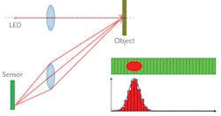
The first case where we see a visible improvement from using the masked point-source LED is in optical signal processing applications. For example, we have optical distance measuring sensors using the triangulation technique. These sensors calculate an object's distance based on a triangulation principle: a light source emits a beam, which is reflected by an object and returns with a specific angle according to the distance of the object.
A linear optical scanner recognizes the intensity of light in different points, generating a curve proportional to the received light in each pixel of the scanner. A signal processor then analyzes this curve and outputs the final result based on the implemented processing algorithm. Figure 3 shows the triangulation distance measurement principle, as well as the ideal signal from the triangulation sensor (separated in pixels).To achieve high resolution and high accuracy, the complexity of the processing must be increased significantly. Sensor pixel size is important for a precise output. Interpolation algorithms are usually implemented as finer data is required and advanced processing is conducted, which requires time and resources at the processing unit. Such processing algorithms are not easily programmed, and demand deep knowledge and experienced engineers.
Even with advanced algorithms, the end result often does not achieve the desired high accuracy. The main source of this problem is the sum of variations that can occur in the system. Because both the light source and the target object have their own variations, the resulting signal in the optical scanner is also irregular and variable (that is, the curve in Fig. 3 becomes strongly distorted).
The masked point-source LED offers a solution for such sensor applications. First, the absence of bond wire and contact shadows creates a completely homogeneous illumination source. Second, the customized aperture size and shape is designed to match the optical lenses, therefore eliminating the unmatched geometries. The resulting illumination has two important properties: 1) well-defined illumination beam area determined by the reticle, and 2) homogeneous illumination distribution confined in the beam area.
These two characteristics are ideal for optical signal processing applications such as the triangulation sensor. With this light source, the signal processor knows that any irregularity is caused by the reflecting object, so more precise information can be obtained about the target, such as the accurate geometry and positioning of the object. This means that the distance measuring sensor with the masked point-source LED can, without as much complexity, calculate more accurate results and operate in more flexible conditions. This results in a high-end sensor with superior characteristics that at the same time simplifies the development and manufacturing processes.
More flexible optical structure design
A second case where masked point-source LEDs can improve the design of a product is with specific optical lens designs. Currently, many systems that require precise optics (such as optical encoders, safety light curtains, and medical equipment) have the design of the illumination source limited by the LED geometry.
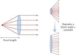
For example, safety light curtains require extremely parallel beams of IR light (to sense objects with finer resolution) with high optical power (enabling greater distances between source and sensor). These requirements are now achieved by using a surface-mount device (SMD) LED chip combined with an optical structure with customized lenses, resulting in a parallel beam with the diameter defined by the lenses. This optical process is called collimation, and fundamental optics theory states that a parallel light is only achieved if the lens and the source are separated by the focal length (this being directly related to the lens and the LED chip sizes).
Another limitation that optical designers face in this situation is the etendue physics law, which states that the light beam cross-section multiplied by the beam angle remains constant. In other words, if you want to reduce the beam angle (approaching parallel light), you need to either increase the beam diameter or reduce the area of the source (see Fig. 4).By providing customized aperture size and geometry, the masked point-source LED aims to remove these design limitations. The possibilities created are extensive, including smaller aperture sizes that enable a shorter distance between LED chip and lenses, and geometry variations that make different lens shapes suitable. In the case of the safety light curtain, smaller lenses and smaller distances are possible, resulting in a more compact product while retaining good light properties.
Goran Pandza is in microsystems and application and Yi Cheng is in applications support in China, both at iC-Haus, Bodenheim, Germany; e-mail: [email protected]; www.ichaus.de.


