MARK S. MILLER and MARYPAT KAVANAGH
The growing demand in environmental and health sensing for inexpensive, low-powered, networked sensing nodes is pushing forward mid-infrared (mid-IR) light-emitting diode (LED) technology and pulling these devices into the market. The mid-IR, spanning roughly 3–12 μm wavelengths, holds a wealth of molecular fingerprint signatures important in many sensing settings.
Smart buildings and smart homes need to monitor carbon dioxide (CO2) for air freshness and volatile organic compounds (VOCs) for maintaining healthy living and working spaces. Outdoors, the oil and gas production and distribution infrastructure needs widespread sensing of methane and other compounds. And wearable and mobile device makers seek new sensors for consumers to monitor their personal environmental exposure and biomarkers in skin.
Valuable gas sensing applications for quantum-cascade lasers (QCLs), interband cascade lasers (ICLs), and quantum-well lasers have proliferated in the mid-IR spectral range. These market developments have in turn propelled the maturation of mid-IR diode laser technology. A large variety of laser devices and assemblies are available from many vendors, providing up to watt-scale powers at some wavelengths.
In contrast, mid-IR LEDs are noticeably early on the technology development curve. These devices have largely been the objects of research. Off-the-shelf commercial devices are available at modest powers and efficiencies, and only at a handful of wavelengths that do not extend farther out than about 4.5 μm.
So, why have LEDs not become widely available in the mid-IR spectral range, especially considering their availability from the ultraviolet (UV) through the visible and into the near-IR spectrum? Has device technology held back applications, or do the applications not benefit from LED properties? Do mid-IR LEDs not offer substantial advantages over thermal light sources—the IR counterparts of incandescent light bulbs—that are mature and widely used for gas sensing? And given these light source disparities, why would a system designer tasked with developing a sensor node not go with lasers for applications that thermal light sources do not already own?
In short, the large-volume Internet-of-Things (IoT) sensor node opportunities come with the constraints of cost and power. LED technologies are especially well suited to meet these constraints, beating lasers on cost and thermal light sources on power.
Mid-IR LED evolution
For the past 20 to 30 years, mid-IR LED development has been pushed ahead at a few outposts around the world.1,2 Just like visible LEDs, the thin light-emitting layers are grown by epitaxy on matched substrates. Pushing an electric current vertically through these layers generates the light.
The light emitted from the surface typically has a broad Lambertian profile beam of about 60° without collimating optics. Emerging mid-IR LEDs use either semiconductor alloys or quantum heterostructures to engineer the light emission using III-V semiconductors in the antimony-arsenide material system, occasionally adding phosphides, on gallium antimonide (GaSb) or indium arsenide (InAs) substrates.
The highest-power mid-IR diode lasers are QCLs. These intraband devices operate with only electrons flowing through the layers and not holes. Unlike other diode lasers, QCLs do not have practical intraband LED counterparts because of high internal losses. Instead, the epitaxial layers used for mid-IR LEDs are based on interband p-n diode structures, where both electrons and holes flow into the device and recombine to create photons.
The output wavelength of the p-n junction emission layer is designed by using either an alloy composition, a quantum well, or superlattice. The superlattices are periodic structures with nanometer-scale layers designed using quantum mechanics.
Alloy-based LEDs have been extensively developed and pushed to near their performance envelope.3 Some of the best long-running alloy LED development has come from the Ioffe Institute (St. Petersburg, Russia) since the 1990s, with a related St. Petersburg firm, LED Microsensor (www.lmsnt.com), offering devices for gas sensing with wavelengths out to about 4.3 μm at continuous-wave (CW) powers of 30 μW. Hamamatsu (Hamamatsu City, Japan) has more recently begun offering alloy LEDs over a similar wavelength range.
Quantum engineering
The superlattice mid-IR LEDs made at Sandia Laboratories (Albuquerque, NM) in the 1990s had early versions of many of the technology features that will likely define the mature endpoint technology, including emission wavelength controlled by superlattice layer thicknesses and p-n emission junctions cascaded by tunneling contacts.4 The tunneling contacts allow a series of p-n diode emission layers to be stacked, and the drive current cascades through the stack of junctions, emitting light at each stage.
Cascading becomes increasingly useful at longer wavelengths, where the smaller semiconductor bandgaps imply lower drive voltages and higher drive currents, at a given power. With cascading, the current can be lowered and the forward voltage matched to the drive electronics.
The newest generation of IR scene generators—which project simulated images for testing IR cameras—use cascaded superlattice LED structures because of their higher performance compared to alloys or quantum wells. For example, the University of Iowa (Iowa City, IA) mid-IR LED group reported outputs of 25 mW when developing mid-IR LED devices based on InAs-GaSb superlattices for scene generators.5
Terahertz Device Corporation (Salt Lake City, UT) offers quantum interband-cascaded superlattice LEDs, called QuiC SLEDs, over the 3-12 μm wavelength range. The LED heterostructure layers are grown by molecular beam epitaxy on GaSb substrates, which are now available commercially as 100 mm wafers.
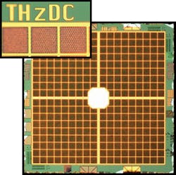
These structures have a few thousand nanometer-scale superlattice layers that provide electron and hole injection and confinement to the light-emitting junctions (see Fig. 1). Electrical current is spread with a metal mesh-semiconductor composite cathode to mitigate the severe current crowding otherwise found for these long-wavelength devices. Within the mesh opening, etched dielectric buttes help extract the light from these high-index materials with n = 3.8-4.0.
The chip format emulates that of high-brightness visible LEDs used for lighting, including a standard backside metallization for eutectic bonding that leverages many supply chain elements of that immense technology base. Small changes in the emitting superlattices are used to adjust the emitting wavelength for a given sensing target, with the rest of the device fabrication staying the same.
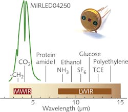
Our TO-39 packaged 4.25 μm QuiC SLED has the output spectrum shown in Fig. 2. The output of this 1 mm die version of our Crestwood LED chip technology lines up with the absorption line of CO2 in the midwave-infrared (MWIR) atmospheric window. Smart Building and medical breath analyzers are important application examples. Terahertz Devices sells these LEDs and matched drive electronics for evaluation, and sells custom die, wavelength, and drive voltage versions of its Crestwood and Silver Lake LED chip technologies.As with other mid-IR LEDs, QuiC SLEDs also serve as good-quality room-temperature photodiode detectors. Our photodiode QuiC (PDQ) fast photodetectors are well suited to LED sensing applications, able to follow short pulses and easily accommodate system power constraints.
Mid-IR LEDs or lasers?
Diode lasers can have exquisitely narrow, stable, well-controlled emission lines for monitoring target species. However, the tradeoffs include device cost, system complexity and cost, and often system power (see Fig. 3). In the mid-IR, diode laser prices are more than an order of magnitude greater than LEDs, albeit with higher power available, as can be seen at the extensive and frequently updated price list at Roithner Laser for hundreds of products.6This price differential reproduces the differentials seen for high-volume commodity devices from the UV to the near-IR, where at a given output power, wavelength, and volume, lasers are typically a factor of 2–50X more expensive.7 The additional greater laser system complexity and power can come in part from the active thermal and optical control needed for stable laser output.
Thermal light sources, hot filaments, and microfabricated heaters have well-established prominent roles in mid-IR gas sensors. These incoherent lights with broad spectral widths and partially collimated beams have enabled applications that include the CO2, carbon monoxide (CO), and hydrocarbon sensors common in automotive exhaust systems, as well as CO2 sensors that monitor patients' breathing in operative and postoperative health settings. Thermal emitters have proved themselves as reliable, low-cost light sources, though modulation frequencies are below 10 Hz and sensor nodes need 100 mW or more from a power supply, constraining battery operation.
The killer LED benefits for environmental and health sensing come from a combination of attributes. The key property separating them from thermal emitters is the ability to drive the LED with short pulses and control the average power with the duty cycle. Thus, even a low-efficiency LED needing 1 W of instantaneous drive power can be driven with microsecond-scale pulses, requiring just microjoule supply pulse energies for the measurement that can easily only require sub-milliwatt sensor node average powers with low duty cycles.
A second contributing key property separating LEDs from lasers is the great cost advantage for the devices, which is amplified by lower system costs. Taken together, these properties enable a new, growing application space for LED-based sensors.
Applications driving LED adoption
All IoT applications require low-cost sensor nodes. Wireless battery or energy-harvested nodes suit indoor and outdoor environmental sensing applications, as well as health and fitness monitoring.
Astonishingly, very recent studies have demonstrated cognitive impairment in people at the low CO2 concentrations previously considered ordinary and safe.8 This matters because smart buildings and homes call for evermore tightly sealed living spaces, needing correspondingly fine-grained sensing and control of air quality, especially since heating and cooling buildings consumes a substantial portion of the total national energy budget. Other gases with pronounced mid-IR signatures, including VOCs and CO, also accumulate in crowded rooms with low air turnover. Mid-IR LED-based sensors are fast becoming important tools in these emerging smart living and working spaces.
Enormous volumes of natural gas products escape into the air every day, especially in drilling and fuel-production settings. The Uinta Basin infrastructure in northeastern Utah has a 10–15% fugitive product loss of methane—a gas being more tightly regulated for its role in global warming.
The immense methane plume from production in the Four Corners region of the U.S. is easily visible from space in IR light. In response, for example, the U.S. Department of Energy has its Methane Observation Networks with Innovative Technology to Obtain Reductions (MONITOR) development program for methane sensing at the wellhead aimed at driving sensing cost per drilling pad to below $3000 per year. Battery-operated, low-cost mid-IR LED sensors certainly have roles in these sensing needs.
Smartphone, smart watch, and fitness band manufacturers face enormous competitive pressures to add sensing features to their devices. Fitness bands and watches already use the LED light absorption of hemoglobin to measure heart rate and oxygenation, re-implementing fingertip pulse-oximeter LED technology used in hospitals. The biomarker targets in the skin for mobile and wearable devices also include blood glucose, which has been successfully measured with mid-IR QCLs, but could benefit greatly from the lower cost and IoT potential of mid-IR LEDs.
Following the lead of CO2 breath analysis in medical settings (called capnograpy)—which itself is transitioning from thermal light sources to LEDs-interest in mobile CO2 monitoring has been mounting.
These emerging applications exemplify how the IoT is ushering in the requirement for stable, low-power sensor nodes for a multitude of applications in homes, schools, workplaces, and for mobile devices. In the same way that sophisticated bandgap engineering has brought QCLs and ICLs to life, it is also dramatically raising the performance of mid-IR interband cascade LEDs.
REFERENCES
1. J. Hodgkinson and R. P. Tatam, Meas. Sci. Technol., 24, 1 (Jan. 2013).
2. N. Zotova et al., Semiconductors, 42, 6, 625–641 (2008).
3. A. Krier et al., Physica Status Solidi, 205, 1, 129–143 (Jan. 2008).
4. R. Biefeld et al., Mater. Sci. Eng. B, 51, 1, 1–8 (Feb. 1998).
5. E. J. Koerperick et al., IEEE J. Quantum Electron., 45, 7, 849–853 (Jul. 2009).
6. See www.roithner-laser.com.
7. See www.digikey.com.
8. J. G. Allen et al., Environ. Health Persp., 124, 6, 805–812 (Jun. 2016).
Mark S. Miller is president and CEO and MaryPat Kavanagh is marketing director, both at Terahertz Device Corporation, Salt Lake City, UT; e-mail: [email protected]; http://thzdc.com.

