ULTRAVIOLET LASERS: UV lasers improve PCB manufacturing processes
The designs of printed circuit boards (PCBs) are pushing the limits of electrical performance in an effort to further the performance and miniaturization of various devices—in particular for consumer electronics such as smart phones, tablets, and GPS devices. With continual advancement in integrated circuit (IC) fabrication, the number and density of connections required to interface to the devices continues to rise.
This trend in turn increases the need for smaller and denser PCB features, including small-diameter micro-vias and high-density interconnect (HDI) patterns. In addition, packaging advances from multichip module (MCM) to ball grid array (BGA) and chip-scale packaging (CSP) continue to decrease the dimensional gap to wafer-level processing.
To meet the materials processing requirements of these designs, ultraviolet (UV) lasers are likely to find increasing application. The energetic photons from UV lasers are absorbed by and cleanly ablate a variety of materials, and the shorter wavelength allows tight focusing—which is beneficial to both fine-feature and high-intensity machining.
Laser via drilling
Via drilling is the gateway application for lasers in PCB manufacturing. Implemented in the late 1980s1 and throughout the 1990s2, the ability of a laser to quickly machine so-called "blind vias"—holes ending at a predefined distance in the PCB material—was a boon for PCB manufacturing. Combined with laminated buildup process advances, it enabled the multilayer PCB architectures that were needed to keep up with the ever-shrinking semiconductor device fabrication node.
The increasing need for small-diameter blind vias for dense packaging applications has created a fast-growing market for lasers. While through-vias in the thickest PCBs are typically drilled mechanically, and CO2 lasers are used for large-diameter blind vias, the smallest-diameter micro-vias found in the most advanced PCB architectures are created with nanosecond-pulse, Q-switched, diode-pumped solid-state (DPSS) lasers in the UV (355 nm) wavelength regime.
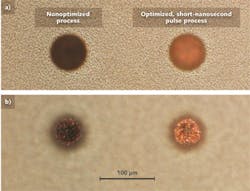
A typical blind-via-drilling application involves removing a few tens of microns of a buildup resin (e.g., ABF or Ajinomoto buildup film) to expose an underlying copper layer. For vias less than about 50–60 μm, the long (~10 μm) wavelength of the CO2 laser is significantly challenged with respect to the ability to focus tightly, and the relatively large melt recast can present additional challenges. In contrast, the clean photoablation that occurs with short-nanosecond, Q-switched 355 nm pulses results in high-quality, melt-free micro-via fabrication (see Fig. 1).
Because of the micro-vias' small size and the strong absorption of the 355 nm wavelength, this application does not require very high pulse energies; just tens of microjoules are sufficient. However, as Fig. 1 shows, a nonoptimal process can give poor results, leaving a copper surface that is unsuitable for subsequent plating. For best quality, short-nanosecond laser pulses and top-hat beam shaping3 are used, resulting in minimal damage/oxidation to the exposed copper surface and minimal sidewall taper, both of which are important for assuring good adhesion of the subsequent copper plating layer.
In Fig. 1, the high-quality micro-via was generated with a Spectra-Physics Hippo 355-5 laser system [5 W power at 50 kHz pulse repetition frequency (PRF)]. While good throughput of about 500 holes/s can be achieved with this laser, a more state-of-the-art via-drilling tool could take advantage of the higher-power UV lasers available today—such as a Spectra-Physics Pulseo 355 nm, 20 W laser—for throughputs approaching 2000 holes/s or higher, depending on via-diameter resin thickness.
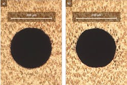
Although drilling blind micro-vias is the primary via-drilling application for 355 nm Q-switched DPSS lasers, a recent generation of higher-power UV lasers is also showing promise for larger-diameter vias in thicker, rigid PCBs. These materials often contain glass fibers in combination with epoxy resins, so high pulse energy and short pulsewidths are beneficial. For example, a Pulseo 355-20 UV laser was recently used for drilling 200-μm-diameter vias in a 2.3-mm-thick copper-clad FR4 material (see Fig. 2).The feature in Fig. 2 was machined at a rate of more than 10 vias/s, which was 2.5× faster than the customer's requirement. Also of note is the high aspect ratio that was achieved: With an exit- vs. entrance-hole diameter difference of just 5 μm over the 2.3 mm thickness, a nearly perfect cylindrical via is formed with a sidewall angle greater than 89.93°.
To achieve the large-diameter, low-taper hole with high throughput, a multiscan trepan routine was executed with a two-axis scanner galvanometer system and a short-focal-length f-theta lens. In addition, precision focus position control was provided with a Newport IMS-V-series high-load bearing linear stage, which adjusted the positioning throughout the cutting process.
Laser-direct patterning for HDI
Micro-via drilling with UV DPSS has aided the march toward smaller, denser wiring patterns in PCB manufacturing. To further this end, the precision machining capabilities of UV lasers are also being leveraged for the wire patterning itself. Current techniques include laser-direct imaging (LDI)4, in which relatively low-power, low-pulse-energy lasers expose the wiring pattern onto a resist material for subsequent chemical etching.
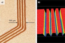
There are now increasing efforts at applying the highest-power UV lasers for laser direct patterning (LDP) in next-generation HDI manufacturing.5 In LDP [also referred to as laser direct ablation (LDA)], there is no supplemental etch process; rather, higher-intensity laser pulses are used to actually ablate grooves in the resin material to the proper depth and width for subsequent copper deposition. LDP processing can easily generate wiring street widths and spacings of 20 μm or less (see Fig. 3)—a number likely to shrink in the future.The features in Fig. 3 were direct-ablated with a scanned, tightly focused Gaussian beam, resulting in processing speeds in the meters-per-second regime. For this approach, a laser with high output power at high PRFs is a good solution, such as the Pulseo 355-Turbo laser system, which offers high power and pulse energy stability at PRFs in the 250–500 kHz regime.
Depending on the beam delivery system configuration—and considering the potential for parallel split-beam processing, etc.—the 20 W output power enables processing of 20-μm-dimension LDP features at speeds beyond 5 m/s. For the smaller feature sizes of the future, significantly higher speeds are possible since more condensed beams can be used, so less energy is required to achieve the same energy density.
PCB depaneling
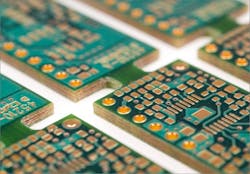
Ultraviolet lasers are used in backend PCB processing as well. In particular, the singulation of finished devices from the PCB panel—a task known as depaneling—is a growing application space. The conventional method is to use a mechanical routing bit. However, manufacturers are looking to increase the depaneling throughput and reduce the cost of consumables (see Fig. 4).While CO2 lasers are suitable for some depaneling jobs, they often leave a significant amount of charring—or carbonization—on the cut surfaces. For many applications, this is unacceptable. For example, from a performance standpoint, problems arise because the carbon products can be conductive and moisture-absorbing, resulting in device failure. In addition, the carbon compounds are strongly aromatic, which is not acceptable for applications in which the product is close to a user's face—such as mobile phones and hands-free Bluetooth headsets.
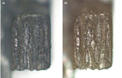
Recently, Q-switched DPSS lasers in the green (532 nm) wavelength have demonstrated good proficiency for various PCB processes, including depaneling of thin-rigid-PCB materials.6 However, for best-quality results with thicker PCBs, tool suppliers are looking toward 355 nm Q-switched DPSS lasers. These lasers are now being offered at power levels and with reliability and pricing that are aligned with the demands of high-volume PCB manufacturing. Furthermore, with careful process optimization, the formation of carbon byproducts can be minimized or avoided altogether with these lasers (see Fig. 5).The depaneling example in Fig. 5 is for an automotive application that must function in an often harsh environment of temperature and humidity extremes. The PCB device board was depaneled with a Pulseo 355-20 laser system. The laser's short-nanosecond pulsewidth and variable pulse frequency allows for controlled heat input into the material. As with many applications, there is a tradeoff between throughput and quality. For best throughput, continuous rapid scanning will cut through the links in a few seconds but with increased carbonization (see Fig. 5a).
If, on the other hand, a best-quality cut is desired, the process is slowed down by introducing cooling delays, which yields lower throughput but low or no carbonization (see Fig. 5b). With short-nanosecond pulsewidths at the 355 nm wavelength, the end user has the ability to tune the process so that the outcome falls at the desired point along the spectrum of throughput vs. quality, depending on the demands of the particular application.
REFERENCES
1. D. Korf, "Laser Drilled Blind Vias Increase PCB Real Estate," Electronic Packaging and Production, 56–57 (1987).
2. L. Burgess, "Multi-depth Blind Vias in Surface Mount Pads for BGA, μBGA, QFP and CSP," IPC National Conference: Solutions for Ultra High Density PWBs (1996).
3. "High-performance Printed Circuit Board Production Equipment for Ultra-high Density Multi-layer Wiring," Hitachi Review, 60, 5, 216–221 (2011); http://bit.ly/V2m2wJ.
4. S. Corbett et al., "A High-Density, Resin-Coated-Foil (RCF) Substrate Utilizing Mask and Direct-Write UC Laser Photolithography," International Conference and Exhibition on High Density Interconnect and Systems Packaging (2001).
5. D. Meier et al., "LDP for Low Cost Flex," Printed Circuit Design & Manufacture, 22, 10, 36 (2005).
6. A. Tamhankar and R. Patel, "New Generation Q-Switched DPSS Nanosecond Green Laser for Efficient Micromachining Applications," Proc. ICALEO 2012, M1306 (2012).
ACKNOWLEDGMENT
Pulseo is a registered trademark of Spectra-Physics, a Newport corporation.
About the Author
Jim Bovatsek
Jim Bovatsek is a senior manager of applications engineering at MKS Spectra-Physics industrial applications laboratory in Milpitas, CA. He has focused on laser applications development using nanosecond, picosecond, and femtosecond pulsed lasers since 2000, with various publications and patents having been generated. He holds a Bachelor of Science (Physics) degree from the University of California, Santa Barbara.
Ashwini Tamhankar
Senior Applications Engineer, MKS Spectra-Physics
Ashwini Tamhankar was senior applications engineer at MKS Spectra-Physics (Milpitas, CA) from 2007 through 2014.
Rajesh Patel
Independent Consultant
Rajesh Patel, now an independent consultant in laser applications, was with MKS Spectra-Physics from 2006 through 2018, with his most recent role there being Director of Strategic Marketing and Applications Engineering.
