Applications for industrial lasers continue to expand
Gary Forrest
Matching lasers to industrial applications has historically required combining output properties of the laser with the economic and environmental factors of industry. The result is an industrial-laser market estimated at $641,000,000 in 1996 with a growth rate of 38% (see Laser Focus World, Jan. 1997, p. 72).
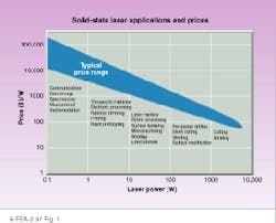
A top priority for any application is the interaction of different laser wavelengths with various materials. A second priority is the power required for a specific function, viewed in light of the importance industrial applications place on throughput. It is not sufficient just to be able to make a part; rather, the number of parts made per hour determines the economic viability of the industrial use of lasers. Figure 1 illustrates the relationship between laser power and specific applications. Also indicated is the current cost per watt and market size for major classes of industrial applications.While cutting, drilling, and welding applications of lasers are well established in industry, newer techniques are both promising great advances and displacing traditional industrial techniques. Two industrial-laser applications that are making rapid inroads on the factory floor—dynamic laser marking and circuit-board fabrication—will be reviewed here. Excimer lithography and annealing of LCD panels, while of great potential impact, will not be considered.
Dynamic laser marking
One of the oldest industrial-laser applications, marking has seen several new developments in recent years. These include tailoring materials for color marking and dynamic marking. Dynamic marking refers to the marking of items as they are moving along a conveyor belt, which has long been the traditional method of marking items with ink or mechanical impressions. For marks that change, ink jet has been one of the preferred methods of dynamic marking, but now as much as 25% of the ink-jet dynamic-marking market is being taken over by laser systems.
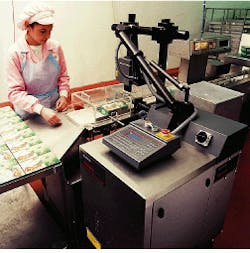
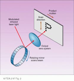
One of these systems is the Lumonics (Oxnard, CA) Xymark. In this system an 80-W CO2 laser is scanned vertically with a rotating mirror and laser "dots" fired under computer control (see photo at top of this page and Fig. 2). The horizontal motion is that of the conveyor belt. The laser control can be synchronized with the conveyer belt to maintain uniform marks. With this approach three to four lines of text can be marked at speeds up to 2000 characters per second.Apart from the technical matching of the laser system to the requirements of dynamic marking, how do the economics match up? Anyone who has used an ink-jet printer can tell you the capital cost of such a printer is typically among the lowest of any printer. But the operating costs are significant because of the consumption of ink. Furthermore, when the ink is used up, the line needs to be shut down for ink replenishment.
On the capital-equipment cost side, a dynamic marker such as the Xymark can be up to twice as expensive, but the consumable cost is nil, and uptime for the system reported by system distributor VideoJet (Clearwater, FL) is 98%. The laser itself has an uptime of 99.5%. To support this high utilization factor, VideoJet offers a full three-year warranty, prorated out to seven years. With minimal disposables and maintenance costs the financial breakeven on dynamic marking is quick for high-volume marking.
On the implementation side, the Xymark is a fully self-contained, mobile unit with a footprint of 24 × 16.75 in. The setup and installation are closely patterned after ink-jet markers. The laser-beam focus is held tight to minimize safety concerns, but retains a greater "depth of focus" than ink-jet printing. On the downside, marking can generate aerosol byproducts, so an evacuator system is needed to remove any volatile or particulate materials generated during marking.
Dynamic laser marking succeeds because it exceeds the economic performance of traditional ink-jet marking and fits into the industrial processing stream with minimal changes in the industrial process.
Circuit-board fabrication
Ultraviolet (UV) lasers have found a solid place on the factory floor for more than 10 years in cutting dielectric materials. Chief among these have been multichip module packaging systems based on excimer lasers. According to Bernd Nikolaus of excimer-laser manufacturer Lambda Physik (Ft. Lauderdale, FL), excimer lasers are factory-floor proven in high-volume, high-precision manufacturing applications such as ink-jet cartridge foil fabrication.
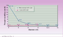
In the past few years there has been increasing interest in UV solid-state lasers, and within the past year the Electro Scientific Industries (ESI; Portland, OR) Model 5100 Laser Processing System has competed successfully against mechanical hole-drilling in circuit-board fabrication. The reason is economics. For holes 8 mil (200 mm) in diameter and smaller, the cost per hole drilled mechanically increases dramatically (see Fig 3). Throughput is lower, and drill breakage is a serious problem. In addition, the very driver for smaller holes (tighter packaging on components on circuit boards) requires higher precision of hole placement—a more difficult task for mechanical drills than laser drills. Mask etching of small holes is also possible but lacks the flexibility of changing hole patterns that the laser-based systems offer.Drilling with UV wavelengths
The UV beam, be it excimer or solid-state, is very well matched to drilling holes in copper-laminated boards. Unlike longer CO2 wavelengths that are poorly absorbed by copper, UV wavelengths are readily absorbed, allowing the laser to punch through the top copper layer without texturing of the layer to enhance absorption. Fortunately, the polyimide absorbs even more strongly, so during polyimide removal the energy per pulse can be reduced (typically to 0.5 J/cm2), and removal of material stops at the next copper layer or a whatever layer is desired. Figure 3 shows an example of a 4-mil (100-mm) diameter through-hole typical of rigid circuit boards made with a 100-J/cm2 trepanned beam cutting through both polyimide and the bottom copper layer. At current laser powers, holes as small as 25 mm can be made at rates up to 10,000 per minute.
One drawback of solid-state UV laser output involves the use of doubling crystals whose long-term use in the high-power industrial world is yet to be fully tested. ESI investigated the removal of polyimide dielectric between copper laminates and found that polyimide removal at 355 nm (tripled Nd:YAG output) was at least as effective as 266-nm output, and at high fluences it was more effective. The UV degradation problems are likely to be much less a factor at 355 nm than at 266 nm, and the output power is higher. Thus, the material-processing requirements for laser circuit-board drilling are actually best met by what should be the more-reliable, longer-wavelength solid-state UV laser.
Some debate still exists over the impact of using very high fluences (>100 J/cm2), with some reports of excess debris generation. According to Alan Cable of ESI, this problem has not been seen in the fabrication of 25-mm holes in circuit boards. He notes that intermediate excimer-laser fluences of tens of joules per square centimeter have shown charring, but because excimer-laser systems are usually configured to drill arrays of holes, very high peak fluences have not been as extensively studied.
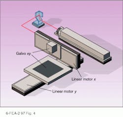
The second requirement is precise hole placement. This is accomplished by combining a large travel stage with on-the-fly galvanometer control of the laser beam placement. The linear-motor x and y stages cover an area of 21 and 25 inches, respectively (see Fig. 4). A synchronized x-y galvanometer then precisely positions the beam over a 20 × 20-mm area with a hole-placement time of less than 4 ms. For typical hole spacings of up to 60 mil (1.5 mm), the two positioning systems can effectively give nonstop coverage over the entire 21 × 25-in. travel.The scanning nature of the solid-state laser beam also lends itself to laser trepanning, in which a larger hole is cut out by scanning a smaller beam in a circle. Likewise, a spiral motion can then be used to remove the polyimide faster from this larger blind via after the copper is removed.
The industrial future
The Precision Laser Machining (PLM) consortium has entered the final two-year phase of a Technology Reinvestment Program to develop diode-pumped solid-state lasers with increased brightness. The commercial impact of this program will be for industrial applications that require very fine beams and high power per unit area. Although the latter may also result in higher throughput speeds, the cost to deliver such high brightness may initially mean that only high-value applications are economically viable. Two such applications demonstrated at TRW (Redondo Beach, CA) are cutting graphite epoxy composites to leave a polished (rather than charred) edge and drilling small holes in titanium and nickel alloys. A 0.001-in. (25-mm) hole has been drilled in Waspaloy used in jet engines to a depth of 0.060 in.
At TRW, the laser most tested to date is a two-times-diffraction-limited 500-W diode-bar-pumped slab laser. Coming on-line this year is a 3-kW laser with a 3.5-times-diffraction-limited beam. Of the two thermal-management issues, diode-bar lifetime seems to be resolved, with tests at SDL (San Jose, CA) reported by TRW to exceed 7000 hours, and Decade Optics (Albuquerque, NM) has continuing tests started in 1994 exceeding 14,000 hours.
The second thermal issue is that of the diode-pumped slab itself. Here, thermal management could directly affect the beam quality required for precision machining and high brightness. TRW reports the stability as "very good," but with the kilowatt laser just coming on-line this year, the final two years of the PLM program will be the critical time to verify that in routine operation thermal management of the slab is acceptable.
In 1997, beta-user test sites are being set up at Utilase Systems (Detroit, MI) for the TRW lasers and at the University of Michigan (Detroit) for the General Electric/Fibertek laser. A handbook is in preparation to assist users in determining the best operating conditions for various materials, and Len Mirabella of TRW notes that they have an internal Internet distribution system for test results.
In the near term, PLM will address specific industrial applications that require high brightness and high beam quality. Current industrial applications will likely be little affected until diode-pumped solid-state lasers have price parity with traditional lamp-pumped solid-state lasers. Industrial system builders are currently looking at diode-pumped solid-state lasers in the 10-W range and finding that the laser price is still too high for industrial applications.
ACKNOWLEDGMENTS
Thanks to Dana Marshall of Cutting Edge Optronics (Bridgeton, MO), Ed Swensen and Alex Cable of ESI (Portland, OR), Natalie Bruton of Lumonics (Oxnard, CA), and Len Marabella of TRW (Redondo Beach, CA) for supplying information for this article. Participants in the Precision Laser Machining consortium are TRW, Fibertek, General Electric Corporation Research and Development, General Electric Aircraft Engines, Hughes Aircraft, Northrop Grumman, SDL, Boeing, Caterpillar, Cummins Engine Company, Newport News Shipbuilding, United Technologies, General Motors, Ford, Chrysler, Process Equipment, Utilase Systems, Edison Welding Institute, University of Michigan, McDonnell Douglas, Opto Power, Spire, Semiconductor Laser International, and Star Medical.
