Optoelectronic devices require light just as electronic devices require current. In today’s technology, the source of that light is semiconductor diodes, either light-emitting diodes (LEDs) or laser diodes. Cheaper but less efficient, LEDs are the most widespread light source for electronic displays, while the main use for laser diodes is fiberoptic communications. (Plasma screens and other less common display technologies will be covered in a future article.) Recent technological developments in both diode technologies are allowing an expansion of the wavelength regions of light produced—into the blue for LEDs and into both blue and medium infrared (IR) for laser diodes.
LEDs—photodiodes in reverse
The basis of LEDs and laser diodes is the same as that for common photodetectors—the photodiode. In all cases, the underlying structure is a p-n junction, the only difference being the direction of the applied voltage or bias. These p-n junctions consist of a layer of silicon doped with atoms carrying extra valence electrons (p-type semiconductors) on top of a layer doped with atoms carrying one valence electron less than silicon (n-type semiconductor). Charge migration creates a depletion region with an electric field directed toward the p region, allowing current to flow in only one direction. In a photodiode, a reverse bias potential is applied across the diode, preventing current from flowing in the absence of light. With exposure to light, electron-hole pairs are created, generating a current.
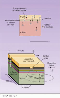
In an LED, the process is exactly reverse. A positive bias is applied, causing current to flow. As the electrons form the n-type semiconductor flow into the p-type semiconductor, they combine with the holes, releasing energy in the form of light (see Fig. 1, top). Because the junctions will absorb light at the same frequency at which they emit it, the junction must be designed so that the emission occurs near the surface, minimizing reabsorption. Nonetheless, the efficiency of LEDs is fairly low, generally less than 10%, and, as in incandescent and fluorescent light, it is emitted equally in all directions. In a typical LED, a 10-µm-thick, p-doped layer of gallium arsenide (GaAs) is applied on top of a 40-µm-thick, n-doped layer, with light emerging from the top surface.Because most of the energy generated must be carried away as heat, keeping the active junction region close to the heat sink, generally the positive metal contact, is important. In the Burrus structure, the substrate is etched away, allowing the light to exit through the “back” and allowing the metal contact to cover the active area entirely, increasing the heat transport and thus the amount of light that can be generated.
An alternative to these surface-emitting LEDs is the stripe-geometry, edge-emitting LEDs, or ELEDs (see Fig. 1, bottom). Here, the active area, the junction, is a narrow stripe, and light is funneled by internal reflection to the edge. The active layers are surrounded on both sides by different semiconductor materials, not just differently doped material, making what is known as a double heterojunction. (An example of this is a GaAs active layer, bounded by gallium aluminum arsenide [GaAlAs].) Because these materials have different refractive indexes, the active layer becomes a waveguide, directing the light out to the edge. In addition, if the doping materials have different bandgaps, as is generally the case, light being refracted through them is not absorbed, cutting self-absorption. As a result, radiance is ten times higher than in the surface LEDs, and, in addition, the output beam is limited to about 30! in width. However, heat-sinking difficulties and more-complex production make these devices more expensive than conventional surface types.
Materials and colors
Just as the bandgap of a photodiode determines what wavelengths it can detect, the bandgaps in LEDs determine the wavelengths of light emitted: the wider the bandgap, the shorter the wavelength. This value is affected both by the semiconductor material and by the dopant used. For infrared wavelengths, gallium arsenide doped with either silicon (910–1020 nm) or zinc (900 nm) is typical. Various compounds of gallium, arsenic, and phosphorus with zinc, oxygen, or nitrogen dopants produce wavelengths between 700 nm (red) and 550 nm (green-yellow). For years, the red LED was virtually the only one used in displays. But since 1993, rapid advances have led to the development of bright blue and true green LEDs, with major technological implications.
Prior to three years ago, the only blue-light LEDs available were those based on silicon carbide (SiC), which had extremely low efficiency, converting the energy of only about three electrons in ten thousand into light. But in December 1993, researchers at Nichia Corp. in Japan announced that they had achieved 3.8% efficiency, 100 times better than with indium gallium nitride (InGaN) operating at 450 nm. By adjusting the indium and nitrogen proportions, they could achieve deep-green operation with similar efficiency at 514 nm. Soon after, Cree Research (Durham, NC) developed another nitride-based device using SiC as the substrate. Because this substrate is a conductor, its small resistance limits heating effects at high current, an important consideration.
In the past two years, research in blue and green LEDs has blossomed, with the addition of ZnTeSe-based LEDs for blue light and ZnCdSe for green light. Improvements in Nichia’s InGaN devices have raised quantum efficiency to 9%, comparable or above that for red LEDs.
The development of efficient blue and green LEDs is of importance, because red, blue, and green are the primary colors used in all full-color displays. LED-based displays may soon be used for flat-panel displays and perhaps eventually flat-screen TVs. In addition, combining red, blue, and green LEDs can produce white light for room illumination. Not only are LEDs longer-lived than standard incandescent bulbs, with 10,000 rather than 1000 hours of life, three-color LED combinations can be adjusted to give the best balance of light, avoiding the yellow light of incandescent and the greenish tinge of fluorescent bulbs. In addition, the new LEDs might compete for such markets as outdoor displays and traffic lights.
At present, the main market for LEDs is, of course, in displays, although over the past decade many of their low-power niches have been taken over by liquid-crystal displays. LEDs are also used for some fiberoptic illumination and communication applications where the high power of laser diodes is not needed. A growing new area of application is emerging in the integration of LEDs into microelectronics circuits, enabling inter- and intrachip optical communication. (This integration will be discussed in a future article in this series.)
Laser diodes—faster, brighter
Laser diodes are similar to LEDs but differ in that the light is generated by stimulated emission rather than spontaneous emission, with the result that the generation efficiency is much higher. To produce stimulated emission, the energy from electrons dropping from the conduction band must be efficiently transferred to the generated photons, because if any significant amount of energy is lost as heat, the resulting photons will have too little energy to stimulate emission from another electron. This limits the materials for laser diodes to those, like GaAs, with direct bandgaps in which the electrons lose energy without momentum being transferred to the lattice. Indirect bandgap structure, as in silicon, transfer of momentum causes the electron to lose energy in the form of heat, and such materials are unsuited for laser diodes.
A second difference between laser diodes and LEDs is that lasers require a higher current. Below the threshold current, self-absorption of the emitted light creates too small a population of excited states to sustain laser amplification: a photon is more likely to be absorbed forming a electron-hole pair than it is to stimulate emission from an excited state. With higher current, the excited states become more populated than the relaxed states—a population inversion. Laser amplification now occurs because each photon on average produces more than one stimulated photon before leaving the laser or being absorbed. Once this laser amplification occurs, the device’s quantum efficiency in converting additional electrical energy into light jumps to values much higher than those for LEDs.
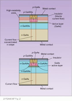
Laser action requires that emitted light be confined and reflected back and forth to form a directed beam. Typically laser diodes use the same structure as stripe or edge-emitting LEDs with the active area being confined on top and bottom by layers with different refractive indexes. The cleaved face at the emitting end acts as a partly reflective mirror, while the other end is generally coated with a reflective coating to produce a fully reflective mirror. Confinement of the active layers from the side is generally accomplished by either gain- or index-guiding (see Fig. 2). Index-guiding simply surrounds the active layers on the sides as well as above and below with material with a different index of refraction, while gain-guiding confines the current to a stripe by blocking off the rest of the device with insulating layers. Index-guided stripes can be made as narrow as 1 µm, leading to nearly all the light traveling in the same direction (although diffraction limitations broaden the beam).It’s not essential that a laser diode be edge-emitting. A newer structure is a vertical-cavity surface-emitting laser. In this design, the active layer is sandwiched below partially reflecting layers and above totally reflective ones. Each laser is exceedingly small, only a few microns across, and millions can be placed on single chip. Their compactness and low threshold current makes them suitable for optical interconnects and optical computing.
Producing a single frequency
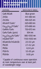
The wavelength of light emitted by laser diodes is, in general, determined by the bandgap of the laser material (see table). Binary compounds have fixed bandgaps, while ternary and quaternary compound bandgaps can be varied within a range by changing the composition. Many of the compounds used for LEDs, as long as they have direct bandgaps, also can be used for laser diodes, as the table shows. However, there is an additional complication—for the high current flows of diode lasers, lattice flaws must be avoided, which means that all the materials in a laser must have nearly identical lattice spacing. In fact, the match between layers and the substrate must be closer than 0.1%.However, the development of “strained layer” technology has allowed the mismatch to increase to 1%, making possible a wider range of materials and wavelengths. A strained layer is a very thin layer, only a few nanometers thick, between two different lattices, which takes up the strain of the mismatch without producing flaws. The necessity of minimizing flaws has also delayed the development of blue laser diodes from the same materials that make blue LEDs. However, it is expected that such production problems will be overcome, so that laser diodes will cover the entire visible spectrum and well into the IR.
Other structures
There are ways of modifying the wavelength of light produced by a given material. The most important is the quantum-well structure, which also improves the general operation of a laser diode. When a layer of material in a semiconductor is made sufficiently thin, less than 50 nm, quantum effects become important because the electrons location is so restricted in one dimension. The result is that the conduction band and valance band split into sub-bands, and the probability of a transition across the bandgap also changes. Because these effects are dependent on the thickness of the layer, changing this thickness can fine-tune the wavelength of light emitted. In addition, a so-called quantum well requires a lower threshold current and has higher gain and a more coherent light output. Although individual quantum wells with small emitting volumes have low power outputs, such layers can be stacked, alternating with inactive layers, producing multiple quantum wells with power comparable to other laser-diode arrays, but with the advantages of quantum wells.
An important modification of the quantum-well structure is the concept of a quantum cascade. In this structure, the transitions are not between the valence and conduction bands but between two conduction bands. The close spacing of these bands allows such lasers to emit light in the mid- to far-IR range.
While any laser diode produces a narrow range of wavelengths and quantum-well lasers are even narrower, a few nanometers (or a few tenths of a percent of the carrier wavelength), even smaller linewidths, around 0.05 nm, are required for fiberoptic communications to minimize dispersion. In addition, the spread of frequencies in the carrier should not exceed 10% of the bit rates, so even for gigabit per second rates, this requires a linewidth of 100 MHz, or about 0.001 nm.
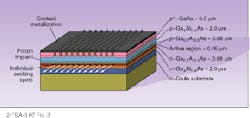
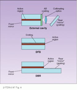
To achieve these very narrow linewidths, some form of grating structure is imposed on the laser cavity to make a single frequency favored over others. In the distributed-feedback laser, a grating structure placed alongside the active layer provides distributed feedback only for the wavelength specified by the grating spacing (see Fig. 4). A distributed-Bragg-reflection laser uses the same principle but places the grating beyond the active layer, connecting them with an optical pathway. Another alternative has the grating as the back reflector to the laser, which allows tuning by tilting the grating. The laser may be separated from the grating by a long external cavity.Laser diodes are not only used for fiberoptic communications, of course. They are currently vital in many applications, including optical recording, printing, free-space laser communication, Doppler optical radar, and medical applications. The continued expansion of the wavelengths produced by laser diodes will inevitably open up new applications in the future.
Eric J. Lerner | Contributing Editor, Laser Focus World
Eric J. Lerner is a contributing editor for Laser Focus World.
