LIDT wavelength-scaling rule of thumb shown to be inaccurate
Optical catalogs often specify the laser-damage threshold of an optic at only one or two wavelengths. This raises the question: What is the laser-induced damage threshold (LIDT) of that optic at other wavelengths? One rule of thumb that has been proposed is that the LIDT can be scaled by an inverse square-root relationship with wavelength: for example, a LIDT measured to be 10.0 J/cm2 at 1064 nm would scale to 7.07 J/cm2 at 532 nm.
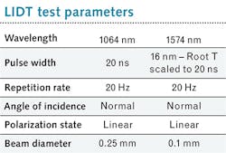
To determine whether or not this rule of thumb is in fact accurate, engineers at Quantel USA (Bozeman, MT), an independent laser-damage testing facility, set out to measure the LIDT of a substrate at different wavelengths. They chose a sapphire substrate with a diameter large enough to allow multiple LIDT tests to be completed on a single surface. The sapphire, which was coated with a dual-band antireflection coating for 1064 nm and 1574 nm, was then subjected to LIDT measurements at both 1064 nm and 1574 nm (see test parameters in the table).
Damage was defined as any permanent laser-induced change observable at 150X magnification with a Nomarski darkfield microscope. The resultant LIDT at 1064 nm was found to be 6.0 J/cm2 (see figure). Using the wavelength scaling equation above, this would correspond to 7.3 J/cm2 at 1574 nm. In fact, the actual measured LIDT at 1574 nm was 15.4 J/cm2, a factor of two higher that the predicted value. The inverse square root relationship was shown to predict a significantly lower LIDT than the actual measured value by more than a factor of two. The Quantel results show that, when needing to determine the LIDT at various wavelengths, the best approach is to measure the LIDT at the wavelengths of interest.
Contact Jason Yager at [email protected].

John Wallace | Senior Technical Editor (1998-2022)
John Wallace was with Laser Focus World for nearly 25 years, retiring in late June 2022. He obtained a bachelor's degree in mechanical engineering and physics at Rutgers University and a master's in optical engineering at the University of Rochester. Before becoming an editor, John worked as an engineer at RCA, Exxon, Eastman Kodak, and GCA Corporation.

