Tunable Lasers: Quantum dots and silicon photonics combine in broadband tunable laser
TOMOHIRO KITA and NAOKATSU YAMAMOTO
A new heterogeneous wavelength-tunable laser diode, configured using quantum dot (QD) and silicon photonics technology, leverages large optical gains in the 1000–1300 nm wavelength region using a scalable platform for highly integrated photonics devices. A cooperative research effort between Tohoku University (Sendai, Japan) and the National Institution of Information and Communication Technology (NICT; Tokyo, Japan) has resulted in the demonstration of broadband tuning of 44 nm around a 1230 nm center wavelength with an ultrasmall device footprint, with many more configurations with various performance metrics possible.
Recently developed high-capacity optical transmission systems use wavelength-division multiplexing (WDM) systems with dense frequency channels. Because the frequency channels in the conventional band (C-band) at 1530–1565 nm are overcrowded, the frequency utilization efficiency of such WDM systems becomes saturated. However, extensive and unexploited frequency resources are buried in the near-infrared (NIR) wavelength regions such as the thousand (T) and original (O) bands between 1000 and 1260 nm and 1260 and 1350 nm, respectively.
Quantum dot-based optical gain media have various attractive characteristics, including ultrabroad optical gain bandwidths, high-temperature device stability, and small linewidth enhancement factors, as well as silicon photonic wire waveguides based on silicon-on-insulator (SOI) structures that are easily amenable to constructing highly integrated photonics devices.1-4
The photonic devices used for short-range data transmission are required to have a small footprint and low power consumption. Therefore, compact, low-power wavelength-tunable laser diodes are key devices for use in higher-capacity data transmission systems that have been designed to use these undeveloped frequency bands, and our heterogeneous tunable wavelength laser diode consisting of a QD optical gain medium and a silicon photonics external cavity is a promising candidate.5
Quantum dot optical amplifier
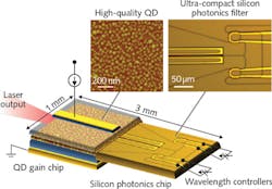
Ultrabroadband optical gain media spanning the T- and O-band are effectively fabricated by using QD growth techniques on large-diameter gallium-arsenide (GaAs) substrates. Our sandwiched sub-nano-separator (SSNS) growth technique is a simple and efficient method for obtaining high-quality QDs (see Fig. 1).
In the SSNS method, three monolayers (each around 0.85 nm thick) of GaAs thin film are grown in an indium GaAs (InGaAs) quantum well (QW) under the QDs. We had previously observed many large, coalescent dots that could induce crystal defects in QD devices using a conventional growth technique without SSNS. Now, we can obtain high-density (8.2 × 1010 cm-2), high-quality QD structures since the SSNS technique successfully suppresses the formation of coalescent dots.
For single-mode transmission, a ridge-type semiconductor waveguide was fabricated for single-mode transmission. The cross-section of the semiconductor optical amplifier (SOA) has an anti-reflection (AR) coating facet to connect a silicon photonics chip with low reflection and a cleaved facet used as a reflecting mirror in the laser cavity.
To fabricate the SOA, the SSNS growth technique was combined with molecular beam epitaxy. Quantum dots comprised of indium arsenide (InAs) with 20–30 nm diameters were grown within an InGaAs QW. Seven of these QD layers are stacked to achieve broadband optical gain. Subsequently, this QD-SOA is used as an optical gain medium for the heterogeneous laser, which can be complemented by other communication technology devices such as a high-speed modulator, a two-mode laser, and a photoreceiver.6,7
Silicon photonics ring resonator filter
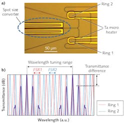
With the QD-SOA fabricated, a wavelength filter is fabricated next using silicon photonics techniques. It includes a spot-size converter that has a silicon oxide (SiOx) core and a tapered Si waveguide that connects the QD-SOA to the Si photonic wire waveguide while minimizing optical reflections and coupling losses (see Fig. 2).The wavelength-tunable filter consists of two ring resonators of different size. The Vernier effect of these two ring resonators allows only light of a specific wavelength to reflect to the QD-SOA. Furthermore, Tantalum micro-heaters formed above the resonators provide a means whereby the laser wavelength can be tuned through application of the thermooptic effect.
Essentially, the wavelength tuning operation of the double ring resonator wavelength filter is achieved through Vernier effects wherein a ring resonator acts as a wavelength filter with constant wavelength interval called the free spectral range (FSR), which is inversely proportional to the circumference of the ring. The tuning wavelength range is determined from the FSR difference of the two rings with FSR1 and FSR2.
A smaller difference in the FSR provides a wider wavelength tuning range, even when the transmittance difference between the main and side peaks is small. On the other hand, a sufficiently large transmittance difference is required to achieve stable single-mode lasing and is obtained using large FSR ring resonators.
Silicon photonics allows us to fabricate an ultrasmall ring resonator with large FSR because of the strong light confinement in the waveguide. The ring resonator consists of four circle quadrants and four straight lines and the radius of the circle was chosen to be 10 μm to avoid bending losses. The FSRs of the ring resonators and the coupling efficiency between the bus-waveguide and the ring resonator are optimized to obtain wide wavelength tuning range and sufficient transmittance difference.
The FSRs and the coupling efficiencies of the double ring resonators are designed to obtain a 50 nm wavelength tuning range and 1 dB transmittance difference. We have since fabricated various wavelength-tunable laser diodes, including a broadband tunable laser diode, a narrow spectral-linewidth tunable laser diode, and a high-power integrated tunable laser diode by using a silicon photonics wavelength filter and a commercially available C-band SOA.8,9
The tunable laser diode
Using stepper motor controllers, the QD-SOA—kept at approximately 25°C using a thermoelectric cooler—and the silicon photonics wavelength filter are butt-jointed (see Fig. 3). The lasing wavelength is controlled by the temperature of a micro-heater placed on the ring resonators. With physical footprints of 600 μm × 1 mm and 1 × 2 mm for the wavelength filter and the QD-SOA, respectively, the total device size of the tunable laser diode is just 1 × 3 mm.Measured using a lensed fiber, the laser output from the cleaved facet of the QD-SOA shows single-mode lasing characteristics with a laser oscillation threshold current of 230 mA. Maximum fiber-coupled output power is 0.4 mW when the QD-SOA injection current is 500 mA.
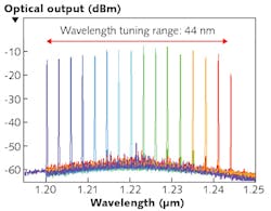
As the ring resonator temperature is increased by a heater with 2.1 mW/nm power consumption, the superimposed lasing spectra show a 44 nm wavelength tuning range with more than a 37 dB side-mode-suppression ratio between the ring resonator's modes. The 44 nm wavelength tuning range of our heterogeneous QD/Si photonics wavelength-tunable laser is, to our knowledge, the broadest achieved to date. The 44 nm tuning range around 1230 nm corresponds to 8.8 THz in the frequency domain, which is far larger than the 4.4 THz frequency that is available within the C-band.Our heterogeneous laser is suitable for use as a light source on a silicon photonics platform that includes other optical components such as high-speed modulators and germanium (Ge)-based detectors. In addition to application as a single-chip broadband optical transceiver for telecommunications, the laser could also be applied to biomedical imaging applications such as optical coherence tomography (OCT), considering the low absorption of NIR light at 1310 nm in the presence of water.
ACKNOWLEDGEMENTS
This research was partially supported by the Strategic Information and Communications R&D Promotion Program (SCOPE), of Japan's Ministry of Internal Affairs and Communications and a Grant-in-Aid for Scientific Research of the Japan Society for the Promotion of Science.
REFERENCES
1. Y. Arakawam and H. Sakaki, Appl. Phys. Lett., 40, 11, 939–941 (1982).
2. D. L. Huffaker et al., Appl. Phys. Lett., 73, 18, 2564–2566 (1998).
3. R. A. Soref, Proc. IEEE, 81, 12, 1687–1706 (1993).
4. B. Jalai and S. Fathpour, J. Lightwave Technol., 24, 12, 4600–4615 (2006).
5. T. Kita et al., Appl. Phys. Express, 8, 6, 062701 (2015).
6. N. Yamamoto et al., Jpn. J. Appl. Phys., 51, 2S, 02BG08 (2012).
7. N. Yamamoto et al., Proc. OFC, Los Angeles, CA, paper W2A.24 (Mar. 2015).
8. T. Kita et al., Appl. Phys. Lett., 106, 11, 111104 (2015).
9. N. Kobayashi et al., J. Lightwave Technol., 33, 6, 1241–1246 (2015).
Tomohiro Kita is assistant professor in the Department of Electrical Engineering at Tohoku University, Sendai, Japan; e-mail: [email protected]; www.ecei.tohoku.ac.jp. Naokatsu Yamamoto is director of the Lightwave Device Laboratory at the National Institution of Information and Communication Technology, Tokyo, Japan; e-mail: [email protected]; www.nict.go.jp.


