Laser Pump Sources: Four 800 kW laser-diode arrays to pump high-pulse-rate HAPLS petawatt laser
Lawrence Livermore National Laboratory (LLNL; Livermore, CA) has installed and commissioned the highest-peak-power laser-diode arrays in the world, which in total produce a peak power of 3.2 MW. The diode arrays, which were developed and fabricated by Lasertel (Tucson, AZ), will act as the primary pump source for the High-Repetition-Rate Advanced Petawatt Laser System (HAPLS), currently under construction at LLNL. When completed, the HAPLS laser system will be installed at the European Union’s Extreme Light Infrastructure (ELI) Beamlines facility, which is under construction in the Czech Republic. The HAPLS is being built and commissioned at LLNL and will be installed and integrated into the ELI Beamlines facility starting in 2017.
HAPLS is designed to be capable of generating 30 fs pulses with peak powers greater than a petawatt at a repetition rate of 10 Hz. The high repetition rate is possible because, unlike existing petawatt lasers, which are flashlamp-pumped, HAPLS is pumped by diode arrays capable of delivering kilojoule pulses at high repetition rates to the final power amplifier.
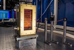
Each laser-diode array supplied by Lasertel supplied contains multiple 888 nm laser-diode bars mounted on water-cooled stacks (see figure). The array operates at a brightness of 10 kW/cm2, which Lasertel notes is a world record, at a repetition frequency of 10 Hz. Each array operates at a total peak power of 800 kW, with four such arrays combined and used as the primary pump sources for the HAPLS laser. More than 500,000 combined laser diode emitters combine to produce the total diode optical input power of 3.2 MW.
“The laser-diode arrays were custom-designed to LLNL requirements,” says Robert Walker, Lasertel’s director of sales and marketing. “The primary parameter that drove the need to customize is the peak power density of the array. LLNL’s laser requires an 800 kW laser-diode array with an emission area of less than 95 cm2. This ultimately translates to a requirement for 500 W peak-power bars in an array of 1600 bars with a bar-to-bar spacing of less than 350 μm. 500 W peak-power bars had been previously demonstrated on a single-bar level, but never in a multibar array. The team at Lasertel developed an entirely new custom laser design that moved the technology from a single-bar demonstration to a 1600-bar array with a peak power of 800 kW at close to 60% electrical-to-optical efficiency in a period of less than 12 months.”
Walker adds that the array assembly includes a bulk optical element that serves as a protective window and several monolithic multibar fast-axis collimation optics.
Pulser power system
The power system, which was developed at LLNL, creates extremely high-current, precisely shaped electrical pulses to drive the diode arrays; each power supply is capable of driving 40,000 A. LLNL holds a patent on this technology.
The power-conditioning system is modular, with a dedicated current driver for each diode stack (one “channel”), explains Walker. “Any channel can be populated (or not) to optimize price/power,” he notes. “Channel waveforms can be individually adjusted to optimize array uniformity. Each driver can deliver over a kiloamp at 100 V compliance, and drivers have been operated up to 20 Hz with the Lasertel arrays and 120 Hz on other systems. It provides 5 μs rise/fall times over 4 m cables.”
The drivers are housed in a common chassis with a DC power-distribution and controls interface. An embedded real-time computer provides control and safety interlock functions. The total system occupies a volume of approximately 0.25 m3, which is about 10 times smaller than typical pulser systems with similar peak pulser power capability.
HAPLS, and other high-average-power, high-energy laser systems enabled by the technologies developed for HAPLS, will drive international scientific research in areas including advanced imaging, particle acceleration, biophysics, chemistry, and quantum physics. In addition, such lasers will be used for national-security applications and industrial processes such as laser peening and others.

John Wallace | Senior Technical Editor (1998-2022)
John Wallace was with Laser Focus World for nearly 25 years, retiring in late June 2022. He obtained a bachelor's degree in mechanical engineering and physics at Rutgers University and a master's in optical engineering at the University of Rochester. Before becoming an editor, John worked as an engineer at RCA, Exxon, Eastman Kodak, and GCA Corporation.
