MICRO-OPTICS: Parallel-optics array monitors sources for data communications
ADAM FEDOR, KATHERINE MORRIS, and JIM MORRIS
Data-communications transmitters based on parallel optics have been used for high-density backplane applications for many years. As the data rate per channel has increased to 5 and then 10 Gbit/s, the number of applications has also increased. Parallel-optics transmitters use vertical-cavity surface-emitting lasers (VCSELs) as the light source and are coupled to a multimode-fiber ribbon cable by using a lens array. Due to the higher data rates now involved, the optical power of each VCSEL in the transmitter must be monitored. To accomplish this, a novel lens array has been developed that monitors each VCSEL in the array while still providing the fiber-coupling, crosstalk, back-reflection isolation, and attenuation values that transmitter manufacturers need.
Vortex diffractive array
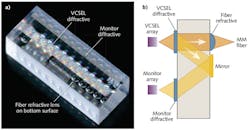
The light from each VCSEL illuminates the lens array, which is called a "vortex diffractive" (see Fig. 1). The vortex diffractive has three functions: It collimates the VCSEL light, taps off and deflects a percentage of the entire beam for the monitor, and imparts a spiral phase to the transmitted beam. The refractive lens focuses the transmitted beam onto the multimode fiber. The deflected beam reflects off an aluminum mirror on the opposite side of the lens array. This reflects the beam onto a second diffractive, the monitor diffractive, which focuses the light onto the monitor photodetector. Most designs have between 1% and 5% of the total power focused onto the monitor photodetector, depending on the design tradeoffs.
The fabrication technique used to manufacture the lens array relies on lithographic processes similar to those used in the semiconductor industry. Fabrication is carried out on 150 mm fused-silica wafers in a cleanroom environment.
The first step of the process involves patterning and etching the diffractive layer. Two additional diffractive layers are patterned and etched to form an eight-phase-level diffractive array. The fabrication process for each layer consists of spinning resist, exposing the resist on a lithographic stepper, developing the resist, and using reactive-ion etching to transfer the resist pattern to the wafer. The diffractive layer typically contains a diffractive element to collimate the VCSEL, a monitor diffractive to focus light onto the detector array, and test gratings.
Each VCSEL diffractive element has a companion monitor diffractive element adjacent to it. A diffractive element with a specified attenuation is then measured to ensure correct etch depth followed by the measurement of diffraction efficiency of the test gratings.
Once the eight-phase-level diffractive array is complete, the fourth step is to pattern and etch the refractive lens array on the bottom of the fused-silica substrate. A second, thicker resist is used to create the refractive lens array using lithography and a reflow process. The back-to-front alignment of the refractive array to the diffractive elements is verified, and the diameter and radius of curvature of the lenses in the array are measured to ensure correct dimensions prior to the transfer etch. The resist is completely etched during the transfer etch, leaving the fused-silica refractive lens array. The radius of curvature and conic of the fused-silica refractive is then verified. A pass/fail wafer map is created from the radius of curvature, conic, and diffractive-efficiency results.
The substrate is cleaned prior to the deposition of the aluminum that will function as the mirror. Resist is lithographically patterned on the side of the substrate with the refractive lens array and the aluminum is then wet etched, leaving only the desired rectangular mirror next to the refractive lens. The metal-mirror alignment is measured to ensure correct placement, and the wafer is inspected to ensure proper completion of the entire process. Because all alignments are performed lithographically, the accuracy is in the micron range.
The wafer is coated with a protective coating and singulated. Once in die form, the parts are picked using the wafer map and a final clean and inspection is performed.
Sensitivity to VCSEL parameters
Coupling of each VCSEL into its associated fiber is affected by changes in the mode structure and divergence of the VCSEL itself. These changes can occur during the operation of the module, as opposed to misalignments, which do not vary much after the module is assembled.
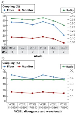
Because changes in VCSEL output affect both fiber-coupled power and monitor power in the same way, the monitor is always measuring the same relative output power of the module, regardless of how the VCSEL is operating. In a simulation of fiber-coupling and monitor power for various Hermite-Gaussian modes, the ratio between the coupled power and monitor power remains relatively constant (except for the most extreme modes), even with multiple different modes (see Fig. 2). When monitor output is compared with fiber coupling for different VCSEL divergences and two different wavelengths, it is seen that the monitor/fiber power ratio is nearly constant over a wide range of VCSEL divergences. Many modern VCSELs are specified for single-mode operation, so this is the most common case.Analyses of crosstalk, temperature effects
A stray-light analysis of the module was created and nominal crosstalk for the monitors simulated. Here, crosstalk is defined as power from all the non-target VCSELs into the target monitor, versus power from the target VCSEL into the target monitor. Crosstalk in the center monitors is worse than in other monitors. Nominal crosstalk was determined to be -16 dB for the center monitors. However, divergence changes in the VCSEL and other tolerances can affect crosstalk as well. Including these effects using a Monte Carlo analysis, we find that crosstalk can typically reach as high as -13 dB. Measurements of an actual module show a crosstalk of -14 dB, well within the expected range.
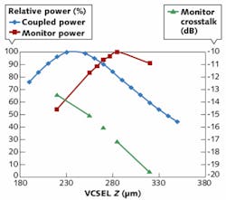
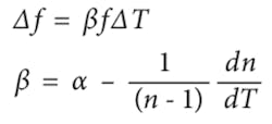
Fiber-coupled power, monitor power, and monitor crosstalk can be plotted as a function of VCSEL z distance (the distance between the VCSEL and the lens array in the light-propagation direction), with the graphs overlaid and normalized so that one can compare the effect of VCSEL z distance on all three values (see Fig. 3). It can be seen that moving the VCSEL farther away from the lens reduces the power coupled into the fiber but also allows potential stray light to spread out further before reaching the monitors, thereby reducing crosstalk.System temperature affects three main aspects of the module: laser wavelength, refractive index, and material expansion. VCSELs typically have a wavelength change versus temperature of approximately 0.6 nm/°C. Refractive-index changes and expansion are characterized by the dn/dT and coefficients of thermal expansion (CTE, α) of the material. For glass, these values are very low (1.28 × 10⁻⁵ and 0.5 × 10⁻⁷, respectively). Using these parameters, one can calculate the change in focal length with temperature for a refractive lens, given by the formula:
For a diffractive element, the change in focal length versus temperature is just 2α. For a 95°C change, this gives about a -1 μm change in focal length for the refractive element and around 0.03 μm change for the diffractive element. Taking into account the laser wavelength change and expansion of the other elements in the system, we get a coupling change of less than 1% over a 95°C temperature range, and monitor power change of less than 0.3%.
The lens array thus allows accurate individual monitoring of every VCSEL channel in an array, while still coupling a majority of the light into a multimode fiber array for transmission. The addition of the monitor function allows the transmitter-module manufacturer to develop closed-loop-feedback control of the laser power while giving the system designer the ability to gather extra diagnostic information from the transmitter.
Adam Fedor is principal engineer, Katherine Morris is senior process engineer, and Jim Morris is senior principal engineer at Tessera Technologies, 3025 Orchard Parkway, San Jose, CA 95134; e-mail: [email protected]; www.tessera.com.


