L. ARTHUR D’ASARO, JEAN-FRANCOIS SEURIN, AND CHUNI GHOSH
High-power edge-emitting semiconductor lasers are used in wide variety of industrial, medical, and defense applications, and are a common choice for pumping solid-state and fi ber lasers. Degradation of these edge-emitting lasers is well known to be dominated by catastrophic optical damage (COD) that occurs because of high optical power density at the emission facet.1 Vertical-cavity surface-emitting lasers (VCSELs), in comparison, are not subject to COD because the gain region is embedded in the epitaxial structure and is therefore not exposed to the outside environment (see Fig. 1). Also, the optical waveguide associated with the edge-emitter junction has a relatively small area, resulting in signifi cantly higher power densities compared to VCSELs. The practical result is that for a typical edge-emitter, the failure rate (the FIT rate defi ned as the number of failures per one billion device-hours) is 500 or higher.2 For VCSELs the FIT rate is on the order of 10 or less.3, 4 This advantage provides a useful lifetime of at least 50 times longer for a system using VCSEL pumps.
FIGURE 1. In a single top-emitting VCSEL device, current and mode confi nement are achieved through selective oxidation of an aluminum-rich layer. The light emits in a circular, low-diverging beam, perpendicular to the epitaxial layers (left). In an edge-emitting laser structure, the light emits parallel to the epitaxial layers in an elliptical beam (right). (Courtesy of Princeton Optronics)
The “activation energy,” EA, is generally used to describe the temperature dependence of the failures associated with a particular technology. This parameter is derived through a plot of the mean time to failure as a function of the inverse junction temperature. In the case of edge-emitters, because COD-induced failure is very sensitive to temperature, their activation energy is typically on the order of 0.45 eV. On the other hand, because VCSELS are not subject to COD, their activation energy is almost twice as high as that of edge-emitters (0.7 eV). This high activation energy means that if only the temperature-dependent term of the FIT relation is considered, VCSELs operating at 80°C are 400 times more reliable than edge-emitters operating at 40°C. We have operated many VCSELs at 80°C for extended periods of time and found no degradation. Others have operated VCSELs at much higher temperatures.5 The ability of VCSELs to operate reliably at higher temperatures is significant because the requirements for refrigeration are much less.
Using these advantages, we fabricated large high-power VCSEL arrays and operated them without a chiller (a refrigeration system that uses a recirculating coolant such as water or ethylene- glycol). The “chillerless” operation of VCSEL arrays results in a more compact laser system with higher overall efficiency.
Array fabrication
To achieve high-power operation with VCSELs, we fabricated two-dimensional (2-D) arrays of single devices operating in parallel. Fabrication of VCSELs is similar to that of well-established low-cost silicon integrated- circuit planar processing. In the case of a VCSEL, the mirrors and active region are sequentially stacked along the epitaxial growth direction. As a result, the light oscillates perpendicularly to the layers and escapes through the top (or bottom) of the device in a circular, low-divergence beam. The VCSEL wafer then goes through etching and metallization steps to form the electrical contacts. Confi nement of both the current and optical emission is typically achieved through either selective oxidation of an aluminum-rich layer, ion implantation, or even both, for certain applications. The VCSELs can be designed for “top emission” (at the epi/air interface) or “bottom emission” (through the transparent substrate) in cases in which “junctiondown” soldering is required for more effi cient heat-sinking, for example.
After processing, the wafer goes to test, where individual chips are characterized on a pass-fail basis. Finally, the wafer is diced and the chips are binned for either higher-level assembly (very high yield, typically more than 95%) or scrap. The wafer is diced into single devices or arrays of single devices effectively connected in parallel. The arrays can be linear (one dimensional), rectangular, or square (2-D). Furthermore, the position of the individual elements in a VCSEL array is defined by photo lithography, which permits arbitrary design layouts of the elements with placement accuracy of microns. Depending on the application, VCSEL 2-D arrays can contain from a few hundred to several thousand single devices.
Because the VCSEL resonant cavity is defi ned by a wavelength-thick cavity sandwiched between two distributed Bragg refl ectors (DBRs), devices emit in a single longitudinal mode and the emission wavelength is inherently stable (approximately 0.065 nm/K), without the need for additional wavelength stabilization schemes or external optics, as is the case for edge-emitters. Furthermore, thanks to advances in growth and packaging technologies, the emission wavelength is very uniform across large VCSEL 2-D arrays, resulting in spectral widths of approximately 0.8 nm. This wavelength stability and narrow spectral width is useful in pumping applications, for example, in which the medium has a narrow absorption band.
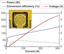
We fabricated 0.22 cm2 VCSEL arrays with more than 230 W of CW output power, corresponding to more than 1 kW/cm2 power density (see Fig. 2). We have also demonstrated more than 100 W of quasi-CW power (power that is pulsed with a pulse width on the order of 100 μs and a duty factor of about 10%) using a higher power density of 3.5 kW/cm2. These values of power and power density are comparable to those of edge-emitters.
null
null
“Chillerless” operation
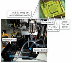
The high-power VCSEL arrays we operated used a cooling system consisting only of a compact radiator/fan and water-pump system, similar to that used in an automobile but on a much smaller scale. The fan/radiator cools water, which is circulated using the water-pump through a microchannel cooler acting as a heat sink under the submount for the VCSEL array (see Fig. 3). In comparison, to operate stacks of edge-emitters a chiller is required . Typical chillers are much larger in size than the radiator/pump system used here for VCSELs. In addition, precise control of the edge-emitter junction temperature is also oft en required to maintain the lasing wavelength at a specific value. Precise control of the VCSEL junction temperature is not required because the wavelength shift with temperature is five times less in VCSELs than in edge-emitters.
FIGURE 3. In a fully assembled high-power VCSEL array, a compact radiator/fan and small water-pump system provide the circulating coolant to remove dissipated heat. Typical chillers for edge-emitting lasers are much larger than the microchannel cooler system used on the VCSEL array (top right). (Courtesy of Princeton Optronics)
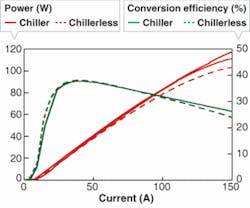
We measured the output power and the power-conversion effi ciency for a VCSEL array operated with a chiller and with the radiator/pump system. The results showed that both the output power and conversion efficiency at the operating point (50 A) for a VCSEL array were essentially the same with the chiller and with the radiator/pump system (see Fig. 4).
FIGURE 4. The power and conversion effi ciency of a high-power VCSEL array remain comparable under two different regimes: operation using a chiller set at a constant temperature of 20ºC, and operation using the small radiator/pump system (“chillerless” operation). (Courtesy of Princeton Optronics)
Even though the conversion efficiency of VCSEL devices is typically less than that of edge-emitters, the use of this radiator/pump system for the VCSEL array results in a significant improvement in overall system conversion efficiency. As an example, in terms of overall system efficiency, a VCSEL device with 48% conversion effi ciency operating with a radiator/ pump has a system-level efficiency equivalent to an edge-emitter device with 65% conversion efficiency operating with the use of a chiller. This is because the chiller power consumption equals the edge-emitter dissipated power ( effi ciency of 1 W/W), while the radiator/pump power consumption is less than 10% of the VCSEL dissipated power, based on actual numbers.
Future prospects
The work described here is based on using indium gallium arsenide/ gallium arsenide (InGaAs/GaAs) semiconductor materials in the active region. Therefore, these results have been at a wavelength of 980 nm. Longer and shorter wavelengths of VCSELs are possible with diff erent III-V semiconductor materials.
Currently, the brightness (defined as the power divided by the square of the beam size times divergence product) for edge-emitters is higher than that for VCSELs. The advantage of edge-emitters in this parameter is that a single edge-emitter can achieve high optical power density (a few watts from a 2 × 100 μm emission area). On the other hand, edge-emitter bars or edgeemitter stacks require complex optics to achieve high brightness. We plan to develop high-brightness high-power VCSEL sources for pumping fi ber lasers and other applications.
In applications in which very large optical output power is needed, such as kilowatts, VCSEL arrays conveniently assemble into “arrays of arrays.” Such structures require only that suitable solders and high-thermal-conductivity submounts be used, such as diamond. Based on our recent results, we believe that VCSELs are now poised to become the technology of choice for high-power laser sources, including pumps for solidstate and fiber lasers.
ACKNOWLEDGMENTS
We are grateful for the support from the DARPA Super High Effi ciency Diode Source (SHEDS) program.
REFERENCES
1. A. Moser, et al., J. Appl. Phys. 71, 4848 (1992).
2. H.-U. Pfeiffer et al., Proc. OFC 2002, 483 (March 2002).
3. U-L-M photonics, “VCSEL Chip Products Reliability Report,” (October 2005).
4. J.A. Tatum et al., Proc. SPIE 3946, 2 (May 2000).
5. R.A. Morgan et al., IEEE Phot. Tech. Lett. 7, 441 (May 1995).
Tell us what you think about this article. Send an e-mail to [email protected].
L. ARTHUR D’ASARO is a senior member of the technical staff, JEANFRANCOIS SEURIN is director of device research and development, and CHUNI GHOSH is chief technology officer of Princeton Optronics, 1 Electronics Dr., Mercerville, NJ 08619; e-mail: [email protected]; www.princetonoptronics.com.


