AL YUEN
Increasing demand for high-power semiconductor lasers will require continual improvements in reliability and cost of ownership. Improvements will be particularly critical for applications that involve high operating temperature and/or on-off operation (temperature cycling), such as direct-diode processes in plastics welding and practical implementations of solid-state laser pumps. Hard-solder techniques and thermal-expansion-matched materials, originally developed for telecommunications lasers, can improve the attachment characteristics of the laser die to the heat sink, resulting in reduced thermal stresses and increased thermal stability-and thus superior device lifetime characteristics under adverse conditions.
Literature on high-power laser diodes is filled with reports of “hero” results with new records for performance and reliability, demonstrating performance that can be achieved under very controlled operating conditions in a laboratory setting. However, designers who incorporate high-power laser-diode bars into their systems often find that commercial product reliability and/or operating conditions limit overall system performance. The culprit in this disconnect between R&D claims and actual results of a commercial device is often the packaging technology used to mechanically support the laser diode and dissipate waste heat, the arch nemesis of intrinsic laser-diode lifetime.
Conventional laser-diode packaging
The traditional packaging approach for high-power semiconductor laser bars is to solder the laser bar p-side (top) down onto a heat sink. The laser junctions are much closer to the top of the die than the bottom, so this geometry minimizes the thermal impedance between the junctions and the heat sink. Copper has been the heat-sink material of choice because its high thermal conductivity maximizes heat flow, thus delivering the lowest possible junction temperature and hence the highest operating power.
Unfortunately, the thermal-expansion coefficient of copper is not well matched to that of the gallium arsenide (GaAs) material that forms the laser. For this reason, soft indium solder is used to bond the two, because its high ductility allows for some differential expansion. This approach delivers excellent reliability for continuous-wave (CW) or quasi-continuous-wave (QCW) operation because the laser bar maintains a steady-state operating temperature.
However, when a device is turned on and off, the repeated thermal cycling subjects the device to mechanical stress because of the the difference in thermal-expansion coefficients. This cycling can lead to material cracking and/or indium migration, either of which can eventually cause failure. This thermal mismatch becomes most critical in “hard-pulse” operation, in which the laser is cycled between on and off states on time scales of about one second. This type of hard-pulse operation is found in direct-diode materials-processing applications, as well as in solid-state pump diodes when it is desired to minimize power consumption or heat dissipation in the laser system. In addition, in solid-state lasers used in military applications, it is typically desired to use elevated heat-sink temperatures (above 50°C) that can cause the indium to soften or even melt.
The hard-solder solution
Technology for mounting a semiconductor laser to a heat sink with similar thermal-expansion characteristics has already been successfully addressed by telecommunications device manufacturers. Low-power lasers produced using this approach have proved to be robust, with extremely long lifetimes (typically over 100,000 hours for a single-emitter device). But there are numerous practical engineering hurdles that must be overcome to adapt this approach to high-power diode lasers. In particular, the die size of a high-power (multi-emitter) laser bar is much larger than that used for single-emitter telecommunications devices. This is an issue because the expansion-coefficient match between the die and heat sink is never perfect, and the resultant mechanical strain is proportional to length. Thus, larger forces must be accommodated.
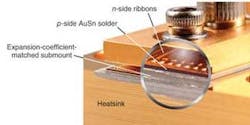
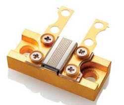
In practice, to implement telecommunications laser-packaging methods in higher-power laser bars several aspects of the process must be modified. Of primary importance, the metallization process must be optimized for the solders and reflow-temperature profiles used. Coherent’s embodiment of this process is called PulseLife solder technology with conduction-cooled package (CCP; see Fig. 1). This process involves placing the semiconductor diode bar on a copper/tungsten heat sink, which provides a relatively good match to the thermal-expansion coefficient of GaAs. The two are bonded using a gold/tin solder that is harder than indium and has a much higher melting point. The n-side of the die is electrically contacted with a ribbon bond specifically designed to carry high current.
null
Performance and reliability
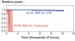
The reliability characteristics of a typical high-power diode-laser bar made using conventional construction methods (copper heat sink and indium solder) can be quantified (see Fig. 2). Specifically, a 40 W bar at 808 nm, having a fill factor of 30%, shows minimal power degradation well past 10,000 hours. In contrast, a similar device-in this case a 50 W laser at 830 nm, also with a 30% fill factor-fails after about 1000 hours when hard pulsed (one-second on/one-second off). Microscopic examination of failed or degraded units subjected to hard pulsing confirms that failure occurred due to indium that migrated into the facet area.
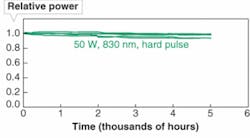
For PulseLife CCP lasers (50 W bars at 830 nm, with a 30% fill factor), preliminary lifetime test results are much improved over conventional packaging techniques (see Fig. 3). The units were cycled one-second on/one-second off. Degradation in output power of less than 10% is seen over 5000 hours of operation. This data was combined with results from three additional life tests from similar lasers with wavelength range between 808 and 830 nm to estimate total device lifetime. Linear extrapolation of this life-test data to a 20% drop in output power yields a lifetime of approximately 26,000 hours.
But what about random failure? This combined data set has 107,000 device hours with one such failure. Using a standard random-failure model, a mean time to failure (MTTF) of 27,600 hours was calculated based on a 90% confidence level.
Similar calculations were performed on data from 980 nm PulseLife CCP lasers with 75 W output power and a 50% fill factor. No device failures were observed within a total of 40,000 device hours, which corresponds to a MTTF of 17,000 hours (90% confidence level), assuming a random-failure model. Modeling long-term degradation, rather than random catastrophic failures, is likely to yield a device lifetime beyond 20,000 hours.
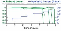
Step stress studies were performed on these lasers to probe the upper limits of the PulseLife CCP platform performance. Both 830 and 940 nm laser bars were hard-cycled at increasingly high current levels, and the current step increases were separated by a few days to a week. The 830 nm lasers generally exhibited good performance up to a current level of 85 A, corresponding to a junction temperature in the 85°C to 90°C range. Examination of the units that failed above this point revealed evidence of catastrophic optical-mirror damage. Devices at 940 nm achieved current levels of about 115 A. This is most probably due to the higher electrical efficiency at longer wavelengths that results in lower junction temperature, combined with lower optical absorption at the facets.
null
Multibar vertical stacks
The use of hard-solder and thermal-expansion-matched submounts also enables the construction of vertical, multibar laser stacks with improved performance and reliability. In the assembly of monolithic or “bar-in-groove” stacks, indium solder is typically used to attach both n and p sides of the laser bar. This “all indium” laser-bar attach is a relatively straightforward process and has the attractive advantage that defective bars can be reworked by simply reheating and replacing the affected bar. However, this “all indium” method has several drawbacks. As in the case of individual bars, the p-side indium is near the facet and is prone to migration, leading to failure; overall lifetime for these lasers is typically in the hundred-million-shot range. In addition, the relatively large gaps needed for solder reflow result in large variations in bar spacing and pointing angle, both of which can impact lensing and subsequent transfer of optical power in the system.
These limitations can be addressed by applying PulseLife solder technology to this monolithic stack construction. This technique uses a grooved, monolithic submount fabricated from copper/tungsten, which provides good matching of thermal-expansion coefficient with the laser bars. Individual laser bars are attached to this submount on the p side using a thin layer of hard (gold/tin) solder. The n-side gaps between bars are then backfilled with a lower-temperature solder.
The PulseLife monolithic stack or G‑stack avoids the bar positioning and pointing issues that arise in “all indium” implementations, yet yields the same reliability benefits as discussed for individual PulseLife CCP bars. These benefits translate into pulse-count lifetimes at the ten billion shot level (which typically corresponds to about ten years under typical operating conditions) for G-stacks composed of bars having an output of 100 W at 25°C. Furthermore, when the PulseLife G-stack technology is combined with a high-temperature laser material technology, such as Coherent’s aluminum-free active-area (AAA) technology, superior reliability and performance can even be sustained at elevated operating temperatures up to 50°C.
Conduction-cooled laser-diode stacks have shown potential in a variety of applications, including pumping solid-state lasers, materials-processing tasks, as sources for localized heat treatment of metals, and even for paint stripping. However, in many of these uses, the laser is subjected to mechanical stress and shock, as well as elevated temperatures, which can limit device lifetime. PulseLife packaging technology shows promise for addressing these concerns, and should lead to wider deployment of high-power diode-laser technology.❏
AL YUEN is director of the Semiconductor Business Unit at Coherent, 5100 Patrick Henry Drive, Santa Clara, CA 95054; e-mail: [email protected]; www.coherent.com.
