Manufacturers boost laser-array production
Modern semiconductor-production techniques increase the volume of diode-array manufacturing and enhance diode-pumped laser development.
Dana Marshall
In recent years, an increasing proportion of commercial Nd:YAG lasers have used diode bars and arrays as the pump source. The major benefits of diode pumping are greater efficiency, lower power consumption, reduced size, lower cost of ownership, increased longevity and reliability, enhanced power, and energy stability. Initially, diode pumping was limited to low-power (a few milliwatt) lasers pumped by single-element diode lasers. Now, lasers with greater than 10 W of output, pumped by diode bars and arrays, are offered by several manufacturers, and industrial kilowatt-level systems are in early stages of development (see Laser Focus World, Sept. 1994, p. 15).
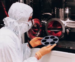
In a typical diode-pumped Nd:YAG laser, the diode pump arrays can represent as much as 30%?40% of the total cost of the laser. In higher-power lasers, this percentage may be even greater. This high cost, together with limited availability, has often forced designers to limit performance for the sake of cost. Adopting modern semiconductor-production techniques, such as multiwafer planetary reactors, enables the production of lower-cost diode arrays in high volume (see photo). The availability of such devices may lead to industrial diode-pumped lasers with higher powers and longer lifetimes.
Design of diode-pumped lasers
The majority of solid-state lasers use Nd:YAG as a gain medium. Its absorption spectrum consists of several sharp peaks and bands. Flashlamps produce broadband light, most of which is, therefore, not absorbed by the Nd:YAG crystal, and this excess pump energy simply becomes wasted heat. The output spectrum of diode lasers is quite narrow, however, and they can be designed to emit only at strong Nd:YAG absorption wavelengths, typically near 808 nm. The result is a much more efficient and compact laser, with solid-state reliability.
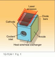
A typical diode-laser array consists of a stack of many (even hundreds) diode bars (see Fig. 1). Each bar is a monolithic semiconductor device consisting of a large number (up to a hundred or so) of active laser junctions. Bar-packaging techniques vary according to the operating performance desired from the array. Cooling can be accomplished by a variety of methods, but most commerical laser systems use some type of water-circulation system for cooling.
Because diode bars typically have represented a large fraction of total laser cost, laser designers have gone to great lengths to deploy them with maximum efficiency so as to require as few bars as possible. This has involved three major design factors: maximizing the output power of the device, efficient coupling of diode light into the Nd:YAG crystal, and temperature tuning of the diode to match the peak absorption wavelength of Nd:YAG.
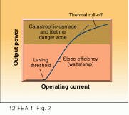
The output power of the bar or array is directly proportional to the operating current above the lasing threshold (see Fig. 2). Higher current, however, reduces the margin of safety below the catastrophic damage limit, the point at which the bar has a greatly increased probability of self-destructing. Some designers operate the diodes at currents that may be dangerously close to this limit. While avoiding short-term catastrophic failure, this maximum-power approach inevitably stresses the device, shortening its lifetime. Because lifetime is such an issue, diode-laser manufacturers are forced to implement exhaustive (and expensive) test programs to ensure that their diodes can survive. Life testing decreases yields and increases diode cost and price.
Designers have used several approaches to efficiently couple the output of bars into the host crystal, often using fiber-coupling and/or lenslet arrays. Both of these configurations require precision alignment of the diode bars with added-on optics, representing a significant material and labor cost.
A typical diode bar emits radiation covering a full width at half maximum of about 2 nm, and the center wavelength is affected by the heat-sink temperature and the average drive current. The primary absorption band for Nd:YAG is only about 4 nm wide, so it is important to provide accurate temperature control when using a small number of diode bars. Scaling to higher-power systems using many diode bars requires elaborate temperature control and diode-bar wavelength-selection trade-offs. The end result can range from extravagant cooling systems to excessively narrow diode-wavelength specifications, both of which can cause system costs to skyrocket.
Slab designs can be different
While these traditional methods attack the efficiency problem, they also increase the system complexity and cost, while decreasing the overall lifetime and reliability of the laser. This design philosophy can be summarized as using the minimum number of precisely selected, thoroughly tested, but highly stressed diode lasers. With the increasing availability of lower-cost diode bars, however, maximizing the efficiency of their use in large industrial systems is no longer an overriding economic issue.
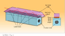
Consider a generic diode-pumped laser design. In medium-power (greater than 10 W) and high-power lasers, side-pumping is necessary because of pumping volume and end-damage considerations. This is easily accomplished with slab geometries using large two-dimensional arrays (see Fig. 3). This scheme is not efficient, nor does it concentrate the pumping energy into a particular mode within the slab volume. It is, however, inexpensive to implement, and with the lower cost of diode bars, the loss of efficiency can be offset simply by using a slightly higher-power diode array (an array with more bars).
Similarly, it is no longer necessary to provide fine wavelength tuning to all the diode bars to exactly match the center of the Nd:YAG absorption band. The arrays can be mounted and cooled together by one low-cost cooling system and can be specified for wider-emission-wavelength bands. Again, the lower efficiency can be offset by using a higher-power array, resulting in a design that is less complex and less expensive to build.
All of these changes, however, do not address reliability and lifetime. Reliability is the most important feature that industrial customers seek in diode-pumped lasers. Extending diode-laser lifetime is most directly achievable by derating, that is, operating the laser at a lower drive current than it is designed to tolerate. This simple change can extend diode lifetimes by a factor of ten. Again, the designer can compensate for the reduced power obtained from each bar by installing more bars. As diode-bar prices decline, this solution is more practical.
Volume fabrication
It has long been believed that diode bars could be produced at commodity prices, given a high-volume market. Catalyzed by market changes, engineers at McDonnell Douglas Corp. (MDC, St. Louis, MO) began a program in 1990 to manufacture very large diode arrays at high volumes and low unit costs. This goal mainly involved implementation of proven semiconductor-production techniques that enabled delivery of more than 5 million peak watts of diode bars between 1991 and 1994.
In 1994, MDC chose to discontinue diode-laser production as part of a core business strategy focused on aerospace manufacturing. Gateway Photonics Corp. (St. Louis, MO), which includes a group of the principals of the MDC operation, was formed late in 1994 specifically to reconstitute this significant production capability.
The basic concept of high-volume diode-laser-bar production relies on a simple shift in philosophy, which is to stop thinking of bars as small lasers. Instead, think of them as semiconductor devices, albeit devices that run at much higher drive currents than most. Aluminum gallium arsenide (AlGaAs) and indium aluminum gallium arsenide (InAlGaAs) diode bars are fabricated with the same basic technologies as silicon integrated circuits and can thus benefit from the mass-production methods used to make silicon devices.
There are several critical aspects to volume diode-laser fabrication. The first was a shift to a production-sized metal-organic chemical-vapor-deposition reactor with multiwafer growth lot capability. This replaced the single-wafer reactors that are in widespread use in laser growth, but which produced less than one wafer per growth run, because part of each wafer was used for testing and material characterization. This meant that wafer processing was to be done using pieces of a wafer.
Multiwafer growth lots allow processing to be done on whole, uncut wafers. This permits the use of standard processing equipment, wafer tracks, and other systems designed for full-wafer cassette operation. Multiwafer fabrication significantly reduces the direct fabrication costs (per diode bar). Processing of matched lots of materials also provides an excellent opportunity for the implementation of comprehensive statistical process control (SPC), which can eliminate entire testing regimens once implemented.
A typical diode laser bar is 8 to15 mm long by 300 to 1200 ?m wide. As many as 1000 bars can be diced from a five-wafer growth lot, and 10 or more growth lots can be conducted in a single reactor-week. Other full-wafer processing steps are performed in multiwafer batches and can keep pace with wafer growth. A processing yield of thousands of diode bars per week is thus relatively straightforward.
After dicing, optical coatings are applied to the diode bars, which are then routed for packaging into one of an assortment of individual bar and array packages. During this phase of production, the diode bar is powered up to obtain wavelength and electro-optical performance data. With high-production volumes and application of good SPC, this testing needs only to be cursory, measuring the variation of bars within a batch and mean performance of the lot. The reduction of exhaustive part screening attacks the single largest cost element of producing diode bars. (Customers such as military and aerospace users will always require 100% part screening and life testing.) The result of implementing these methods has been a steady decrease in the cost of bars and arrays. Quasi-CW bars are now available for only about $3/W in production quantities.
In early personal computers, memory was a scarce and expensive commodity, causing designers to carefully write code that made efficient use of memory. Today, this equation has been reversed; memory is essentially a commodity item, and software designers concentrate solely on adding performance and functionality. With the advent of low-cost diode arrays, this same transition is now taking place in the design of diode-pumped Nd:YAG lasers. This trend will continue to produce lasers that are more economical, compact, and reliable and will ultimately lead to their use in a much broader range of applications. n
Planetary reactor allows batches of multiple wafers containing diode lasers to be fabricated
simultaneously, thereby increasing yields and theoretically lowering costs.
FIGURE 1. Two-dimensional diode array
consists of a stack of several diode bars.
FIGURE 2. Output power of a diode laser increases as operating current is increased, but, for long lifetime, laser output should remain below catastrophic damage zone.
FIGURE 3. For high-power output, the simplest way to couple light into a slab is to side-couple the diode pump arrays against the sides of the laser crystal.


