European firms take the lead in high-precision micromachining applications
Given its long history as a dominant force in the machine-tool and materials-processing industries, it should come as no surprise that Europe is also at the forefront of micromachining technology and applications. A number of advances in femtosecond and picosecond lasers will be showcased at the Laser Precision Microfabrication symposium during Laser 2003 in Munich, Germany, this month, along with new applications enabled by these advances.
"With the advent of easy-to-use solid-state lasers and reliable excimer-laser systems, micromachining applications have grown continually," said Andreas Ostendorf, executive director of the research facility Laser Zentrum Hannover (Germany) and co-chair of the LPM symposium. "With the addition of ultrafast lasers, nearly all materials can now be processed, which is very important as the variety of materials in micromachining is orders of magnitude higher compared to sheet-metal welding or cutting in the transportation industry."
According to Ostendorf, in Europe the use of lasers for micromachining has been driven primarily by the major electronics firms—Siemens, Philips, Matsushita, IBM, and Thales—and the premier machine-tool firms, including Trumpf and Rofin-Sinar. While these companies already use or supply lasers regularly for the fabrication of printed circuit boards, integrated circuit packaging, sensor trimming, and repairing lithography masks, there is also a growing trend to outsource many of these applications to job shops that specialize in laser micromachining.
Several technology advances are helping to fuel this trend. In particular, European manufacturers of nanosecond, femtosecond, picosecond, and excimer lasers are building more robust, compact, and affordable lasers that can withstand the demands of an industrial environment. As a result, these lasers are finding use in applications for which they previously were not suited, such as the drilling and marking of automotive and aircraft parts, microelectronics, and biotechnology products. They are also being used increasingly in semiconductor chip manufacturing for silicon and sapphire wafer cutting and scribing, and by the LED and display industries for micropatterning and machining of backplanes.
Much of this work has been spearheaded by government-sponsored projects at European R&D facilities, such as Laser Zentrum and the Fraunhofer Institute for Laser Technology (ILT; Aachen, Germany). For example, ILT is currently involved in the Fraunhofer Alliance for Modular Microreaction Systems (FAMOS) for the biotech industry, with ILT supplying microstructured reactor components made from plastics, metals, and ceramics. Excimer and frequency-tripled Nd:YAG lasers are used to process plastic and ceramic components; Nd:YAG lasers are used to cut, weld, and ablate stainless-steel components; and diode lasers are used to bond plastic parts.
In addition to marking, microjoining, cutting, drilling, and ablation, ILT director Reinhart Poprawe said many exciting new microfabrication applications are emerging, including laser-induced adjusting, where local thermal effects are used to adjust material in products such as microelectromechanical devices and sensors; polishing, in which short-pulse lasers reduce the surface roughness of nonflat objects; and laser-selective melting for rapid prototyping. To enable these new applications, researchers are working on ways of improving existing lasers and developing new types of sources.
Taking it to the streets
One of the major advantages of industrial R&D projects in Europe is that they almost always involve commercial partners, so that technology and application development is done with an eye on what the market needs and what it can afford. This has most definitely been the case with laser micromachining. As a result, European companies are now marketing several ultrafast micromachining lasers, and several startup companies are launching next-generation products.
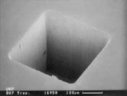
FIGURE 1. Because of the "athermal" ablation effects of the short-pulse 150-fs Thales Bright laser, lasers can now be used to drill transparent materials such as glass without creating cracks or inhomogeneous molten zones around the focus spot.
One of the commercial leaders in ultrafast industrial lasers is Thales Laser (Orsey, France). The company offers a range of diode-pumped solid-state nanosecond lasers in the 266- to 1064-nm range for applications such as selective thin-film removal and high-precision microdrilling. These second-harmonic multimode Nd:YAG lasers offer pulse repetition rates up to 30 kHz and output powers up to 100 W and are used in marking, microcutting, thin-film patterning, and hole drilling of silicon, stainless steel, copper, glass, and silica for products ranging from integrated circuit boards to cardiovascular stents (see Fig. 1).
"Working at the second harmonic not only allows smaller focal spots but also gives access to the micromachining of a number of materials that do not absorb light in the infrared, such as copper," said Antoine Duret, technical marketing engineer at Thales. "Moreover, the short wavelength results in a much more ablative effect than the first harmonic of CO2 lasers, diminishing dramatically the thermal effects that often limit the quality of a feature."
Thales also offers femtosecond lasers for micromachining and has worked to make these lasers easier to use and maintain. According to Duret, femtosecond lasers offer several advantages over nanosecond lasers for micromachining, including reduced thermal effects and features down to 100 nm. In addition, femtosecond lasers can drill or cut glass without any cracks at kilohertz rates. The biggest obstacle has been in making them more suited to industrial applications outside of the laboratory.
"Femtosecond lasers have historically been complicated systems dedicated to scientific research, and advanced skills in lasers were necessary to use them," Duret said. "But in the past few years, thanks to the work of many research teams, scientists have started to bridge the gap between scientific and industrial use. Consequently, industrials are showing growing interest in femtosecond lasers for emerging micromachining applications."
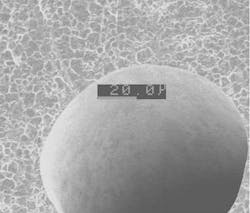
FIGURE 2. Picosecond lasers can be used to micromachine metals with the same quality as femtosecond lasers, but faster. Researchers at the Institut für Strahlwerkzeuge used a forerunner of the Lumera Staccato laser to drill this 1-mm-thick stainless-steel sheet.
Even with these advances, however, some laser manufacturers believe that femtosecond lasers are still limited in terms of micromachining applications and have instead turned their attention to excimer and picosecond lasers for this market. Lumera for example, is launching a series of compact solid-state picosecond lasers specifically for industrial applications such as micropatterning thin films and machining millimeter-thick steel (see Fig. 2). According to Bernhard Klimt, director of marketing and sales at Lumera (Kaiserslautern, Germany), the newest of these is Staccato, a diode-pumped Nd:YVO4 laser that delivers pulse energies up to 400 µJ in 15-ps pulses at a repetition rate of 50 kHz.
"The Staccato micromachines metal with the same top quality as femtosecond lasers but does it with less investment and about 20 times as fast," Klimt said. "The laser's peak power density of more than terawatts per square centimeter allows virtually any material to be machined."
According to Klimt, harmonics at 532, 355, and 266 nm will be available shortly. The Staccato will be demonstrated at Laser 2003 in a micromachining center from 3D Micromac. Lumera also offers picosecond lasers at 532 nm (up to 20 W), 355 nm (up to 7 W), and 266 nm (1 W) at a 160-MHz repetition rate for micromachining thin films and quasi-continuous-wave applications such as direct writing, direct imaging, digital printing, fluorescence imaging, spectroscopy, laser pumping, and materials research.
Application decides the laser
Others believe the excimer laser offers a more affordable, reliable, and precise solution for certain micromachining applications. Incorporating many of the same features as the excimers used in microlithography, including solid-state switching and corona preionization, TuiLaser (Munich, Germany) has developed a compact, low-cost excimer laser for high-precision industrial applications. According to Heinz Huber, sales and marketing director at TuiLaser, the system is only half the size of a suitcase but offers 20 mJ/pulse, with repetition rates up to 2 kHz, and 10 to 40 W of output power—and at a cost of only $30,000 to $70,000.
The advantage of the excimer, Huber says, is that its nonthermal effects make it perfect for marking and machining plastic, glass, crystal, and other materials that might melt or crack if a different laser were used. Thus, TuiLaser is finding niches for its system in such areas as biotechnology and medical-device manufacturing, in which the nonthermal precision of the laser makes it possible to drill 30-µm-diameter holes in plastic nozzle tips or capillaries, for example, or to etch 20- to 50-µm-deep channels in polycarbonate sheets for "lab-on-a-chip" applications.
"In micromachining, laser ablation is the underlying process," Huber said. "The smaller the penetration depth is, and the faster the pulse, the more the ablation takes place without destroying underlying surfaces. With the excimer, the pulse width is short (10 to 20 ns) and the wavelength is short, so the penetration is very small and there is high absorption. This gives you an ablation that is very shallow and causes no thermal damage."
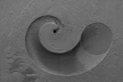
As a microfabrication systems integrator, Exitech (Oxford, England) is in a unique position to offer its customers all of these lasers, and more. In fact, according to Adrian Baughan, sales and marketing manager, when it comes to micromachining, it is not so much an either/or but rather a matter of matching the most appropriate laser to the application. Exitech works with a number of laser suppliers to develop both the systems and the applications for these products. For example, Exitech has become known as an expert in microscopic drilling applications, such as drilling microvia holes for printed circuit boards, where the company's dual-laser system (excimer and CO2) can create 10,000 complete holes/s. Exitech laser systems have also found a niche in synchronized image scanning for backplanes and plasma screens (see Fig. 3).
The company also sells a variety of solid-state laser systems for the microfabrication of MEMS devices, microfluidics, and even inkjet printer heads and has developed a technique for pixel-scale patterning of thin films for liquid-crystal and organic light-emitting displays (OLEDs) and plasma screens that is now being adopted by most of the major display manufacturers. This technique involves a high-repetition-rate diode-pumped solid-state (DPSS) laser to remove a layer of indium tin oxide from the substrate (glass) without touching the substrate and creating thousands of 200- to 250-µm pixels per second in the process. According to Baughan, this approach replaces a much more complicated and expensive multistep chemical-etching process commonly used in plasma-display manufacturing.
In addition to its success in the display industry, Exitech has found an emerging market for its scribing and cutting systems in the production of solar panels and photovoltaics. Here a dual-wavelength system (1064- and 532-nm DPSS laser) is used to scribe the silicon wafers and make circuits for the thin films. As with the pixel-patterning technique used in display manufacturing, 1064-nm is used to remove the indium tin oxide from the substrate, and the 532-nm laser is used to remove the other layers.
"Our core competency is in the application of the lasers," Baughan said. "Our biggest market right now in terms of revenues is lithography, but that is because the machines are very expensive. In terms of future business and most machines being sold, displays and solar panels are becoming our largest markets."


