LIGHT-EMITTING DIODES: Silicon is foundation for LED display

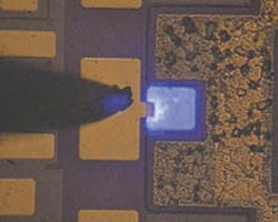
Although mass production has brought down the cost of active-matrix liquid-crystal displays, forming the required transistors and transparent conductors on glass substrates makes for a complex process. A flat-panel display that could be made on a silicon (Si) wafer would take advantage of the more-straightforward Si-based processes developed by the integrated-circuit industry, as well as the industry's large infrastructure. Researchers at the University of South Carolina (USC; Columbia, SC), the Materials and Manufacturing Directorate (Wright-Patterson AFB, OH), and Sensor Electronic Technology (Troy, NY) have moved toward this goal by fabricating blue light-emitting diodes (LEDs) on a Si substrate (see image on p. 16). The LEDs are made from gallium nitride/indium gallium nitride (GaN/InGaN).
The researchers make use of a combination of molecular-beam epitaxy (MBE) and low-pressure metal-organic chemical-vapor deposition (MOCVD). First an aluminum nitride buffer layer is grown on a Si wafer using MBE, after which a GaN layer is deposited via MOCVD. Next comes a 0.2-µm layer of silicon dioxide (SiO2), which is patterned with 300-µm-square holes using standard photolithographic procedures. It is the array of holes that allows for the selective-area patterning of the LEDs. All subsequent semiconductor layers are deposited within the holes using low-pressure MOCVD; the deposition conditions do not allow nitride to be deposited over the SiO2.
The LEDs emit at a peak wavelength of 465 nm, with a 40-nm spectral bandwidth at full width at half maximum. Their forward differential resistance is a factor of four higher than high-quality GaN/InGaN LEDs grown on a more-conventional sapphire substrate; further work is needed to find the cause of the increase, say the researchers. Their light output is a factor of five less than GaN/InGaN LEDs on sapphire. "These are initial devices," says Asif Khan, a professor of electrical engineering at USC. "We are working on optimizing the devices and improving their quantum efficiency." Lifetimes of the LEDs on Si are expected to be as good as for similar LEDs on sapphire, notes Khan.
The researchers successfully tested the LEDs to temperatures of 250°C. The peak emission wavelength lengthened slightly with increasing temperature, and the intensity dropped by a factor of ten as the temperature increased from 25°C to 250°C. In addition, the linewidth broadened to 50 nm at 250°C.
Coming next are green GaN/InGaN LEDs, according to Khan. He expects them to have the same linewidth as the blue LEDs. "In principle, it is not more difficult to make amber LEDs on Si than on sapphire," he adds. "However, we have not tried this yet." Khan says it should be possible to produce a two-color display very soon.

John Wallace | Senior Technical Editor (1998-2022)
John Wallace was with Laser Focus World for nearly 25 years, retiring in late June 2022. He obtained a bachelor's degree in mechanical engineering and physics at Rutgers University and a master's in optical engineering at the University of Rochester. Before becoming an editor, John worked as an engineer at RCA, Exxon, Eastman Kodak, and GCA Corporation.