Alvin Compaan
Thin-film photovoltaic (PV) coatings on inexpensive substrates have long held great promise for reducing the cost of solar energy. This promise is now being realized with simultaneous advances in three separate thin-film PV technologies, one based on hydrogenated amorphous silicon (a-Si:H), one on copper indium diselenide (CIS), and the third on cadmium telluride (CdTe). In each of these technologies, high-rate laser scribing is a key step in moving from small cells to the monolithic integration of cells into large-area panels. Although the dimensions in PV cells—with 50- to 100-µm-wide scribes 1 to 2 cm apart—are much different from those of monolithically integrated silicon chips—with their smallest features at 0.25 µm—their integration is nevertheless monolithic in the sense that a large number of PV cells are interconnected on a single substrate and this is accomplished as an integral part of the manufacturing process.
Why is series integration of cells into modules needed? Sunlight falls on the earth's surface with an intensity of about 1 kW/m2, so that a 1-m2 solar cell operating at 10% efficiency is capable of producing about 100 W of electrical energy. The cell current scales with its area, but its output voltage is typically about 60% of the bandgap energy of the semiconductor material, measured in electron volts. Thus, typical output voltages are 0.6 V for Si and CIS, 0.8 V for CdTe, and 1.0 V for a-Si:H. This voltage is independent of the cell area, so a 10% efficient CdTe cell of 1 m2 producing 100 W of power would develop 125 A of current, because electrical power is the product of current and voltage. For current this high, the current-carrying bus lines would need to be prohibitively thick; also, the transparent conducting oxides, used for one of the electrodes in each of the thin-film technologies, are too resistive.
The solution is to cut the film into smaller cells and provide series interconnections. This way, the same 1-m2 film with 100 integrated cells would produce only 1.25 A at 80 V but yield the same power as the larger cell. The challenge is to achieve the interconnections with the smallest possible loss of thin-film real estate. Rather than using individual hand- or machine-wired connections, as is done for Si PV wafers, this should be done monolithically during the fabrication of the panel.
Scribing interconnections
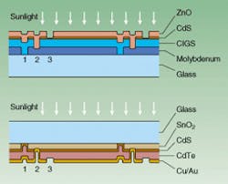
The classic interconnection is a three-scribe series, although variations on this scheme are possible.1 Note that in the context of thin-film photovoltaics, scribing really means cutting completely through one or more layers and not just marking the surface prior to cleaving, as is the case for Si wafer scribing. The first scribe divides the conductive coating on the glass into isolated stripes. The second scribe, done after deposition of the semiconductor layer, provides the interconnect path, or via, through which the final conductive coating contacts the first electrode. The third scribe cuts the top electrode to isolate the cells and complete the fabrication into a series-interconnected structure. This three-scribe pattern is repeated every centimeter or so (see Fig. 1).A successful interconnection must have both low series resistance and high shunt resistance. Residual semiconductor material or an oxide layer left at the bottom of the via will lead to unacceptable series resistance. Shunting will occur if occasional bridging material is left after either of the isolation scribes (number one or three), because these two layers are highly conductive.
Because the space between scribes one and three does not provide active current generation, it is important to achieve reproducible and clean scribes and to keep them as tightly packed as possible. Furthermore, at the PV module production rates planned for facilities recently built or under construction, the overall linear scribe speed may need to exceed 10 m/s. Laser scribing may be the only feasible process for meeting these requirements (see photo at top of this page).
Making cuts
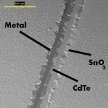
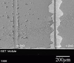
At least three possibilities exist for producing the thin-film cuts needed. Photolithography followed by wet chemical etching has been discarded as too slow and environmentally unfriendly, especially for the large total areas needed for PV. Mechanical scribing has been used successfully and may be acceptable for some of the PV layers in medium-volume production. Scribing with pulsed lasers, however, is rapidly becoming the tool of choice in the PV industry.Mechanical scribing with the use of a diamond-tipped stylus or appropriate blade can work for the softer semiconductor materials—such as CdTe, copper indium gallium diselenide (CIGS), and a-Si:H—if the process does not damage the underlying layer (see Fig. 2). Tearing of the film is a particular problem for films such as zinc oxide (ZnO) that have low adhesion (see Fig. 3). Furthermore, complete removal of a semiconductor, such as SnO2:F, from a rough surface with high haze can be difficult. Mechanical scribing of harder films such as molybdenum on glass invariably leads to scoring of the glass, which then contributes to increased risk of breakage in subsequent processing.
Most of these problems do not occur with laser scribing. Our group has recently completed a survey of laser systems applied to the thin-film materials used in the CdTe-based and CIS-based PV modules.2 We made only limited measurements in a-Si:H-related materials, which were not the focus of our study. We have found that good scribes can be obtained with a wide variety of pulsed lasers, such as Nd:YAG (lamp-pumped, diode-pumped, Q-switched, and modelocked), copper-vapor, and xenon chloride and krypton fluoride excimer lasers. It is important when choosing a laser, however, to pay attention to the specific material properties (absorption coefficient, melting temperature, thermal diffusivity, and so on) of the films used in the solar cells.
YAGs and excimers
For most materials, with the notable exception of ZnO, we could obtain good scribes with the fundamental or frequency-doubled outputs of Nd:YAG lasers. Reliability, stability, serviceability, and cost of operation point toward the selection of a diode-pumped Nd:YAG or Nd:YLF laser as the scribing engine of choice. Remarkably, both the fundamental and doubled wavelengths work well on the transparent conductor SnO2:F, even though its absorption edge lies at about 340 nm; free carriers and defects apparently provide enough absorption to initiate the scribe. We found that ZnO:Al is difficult to scribe with 532- and 1064-nm pulses, but we expect that frequency-tripled or -quadrupled Nd:YAG should work for ZnO. Both of the excimer lasers tested worked very well for ZnO. In fact, they produced excellent scribes in all of the materials tested.
The thin-film PV coatings are typically put on substrates with poor thermal conductivity. Partly because pulse duration is not a strong parameter in the vaporization process—pulses shorter than 5 ns appear to provide no advantage for scribing of these materials in thicknesses ranging from 1 to 5 µm. In fact, it is somewhat more difficult to obtain deep scribes with the shorter pulses because of higher nonlinear absorption at the surface and in the plume—consequently, pulse-energy density rather than peak-power density determines the condition for most-efficient scribing. Naturally, higher pulse-energy densities are needed for wavelengths that have lower absorption coefficients. This is most noticeable for scribing of the transparent conductors SnO2 and ZnO, as well as for CdTe with the Nd:YAG fundamental, because CdTe is transparent at 1064 nm.
As a rule of thumb, most-efficient scribing occurs at energy densities about ten times the threshold for surface damage. The use of higher energy densities at the center of the focal spot leads to wide heat-affected zones surrounding the scribe. These heat-affected zones often lead to poor electrical properties in the semiconductor films, due to defects and deviations from stoichiometry.
An example will illustrate the application: A typical pulse-energy density for scribing is 5 J/cm2 for many of the thin-film materials. A 30-µm-diameter focal spot thus requires about 35 µJ per pulse. Because a typical diode-pumped Nd:YAG laser may deliver 1 mJ per pulse, the application calls for either division into multiple beams or the use of cylindrical focusing. At the other extreme, an excimer laser with 400 mJ per pulse permits the formation of a line image across the entire width of the PV module. This configuration would allow special control of the spatial parameters, tailoring the shape of the scribe and reducing the power as the multiple-pulse scribe approaches the interface with the underlying layer. Such control achieves a clean, self-limiting scribe depth.
Although pulse duration is a secondary parameter, there is one case in which the use of a long pulse is advantageous. A pulse duration of 250 ns or more (achievable with Nd:YAG lasers at high repetition rates) appears to be the most desirable condition for scribing CIS on top of molybdenum. Because of the high melting temperature of molybdenum (2896 K) and its relatively high thermal diffusivity (0.54 cm2/s) compared with CIS (Tm = 1600 K; D = 0.022 cm2/s), the scribe through the CIS can be self-limiting for a carefully chosen energy density.2
As the thin-film PV industry gears up to high-volume production of large solar panels, high-repetition rate, high-reliability, low-maintenance pulsed lasers are the consensus choice for achieving the compact interconnects with high electrical performance that are critical to large-area PV panels.
ACKNOWLEDGMENTS
The author would like to acknowledge First Solar LLC (Toledo, OH) and International Solar Electric Technology (ISET; Inglewood, CA) for assistance with the PV aspects, Spectra-Physics Lasers (Mountain View, CA) and Lambda Physik (Ft. Lauderdale, FL) for access to their applications laboratories, and the support of the National Renewable Energy Laboratory (Golden, CO).
REFERENCES
- S. Wiedeman, R. G. Wendt, and J. S. Britt, AIP Conference Proceedings Series # 462 (1999).
- A. D. Compaan, I. Matulionis, and S. Nakade, "Optimization of Laser Scribing for Thin-Film PV Modules," Final Technical Progress Report, NREL/SR-520-24842 (available from NTIS).
ALVIN COMPAAN is a professor of physics and director of the Center for Materials Science and Engineering at the University of Toledo, Toledo, OH 43606; e-mail: [email protected].


