Telecom is benefiting from the advantages of VCSELs, but the need for high gain and current density make heat-sinking and high-temperature operation important issues.
Telecommunication represents one of the biggest markets for high-performance semiconductor diode lasers. Telecom applications have been traditionally dominated by the superior output power of edge-emitting devices, but vertical-cavity surface-emitting lasers (VCSELs) are emerging as a low-cost alternative for that application.
The most expensive step in the fabrication of lasers is the delicate procedure of cleaving and mounting the die to a proper heat sink and then packaging it for better handling. An edge-emitting device can only be tested for compliance with customer specifications at the end of the manufacturing process, whereas VCSELs can be processed and tested on a full-wafer scale. Because the emission is parallel to the direction of growth of the semiconductor layers and perpendicular to the surface, no cleaving is necessary and the output signal of the laser remains accessible. The ability to test earlier in the process, allows the manufacturer to package only those devices that meet specifications, significantly reducing final device cost.
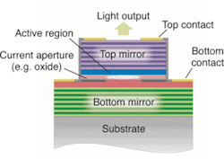
FIGURE 1. In a cross-sectional view of a VCSEL, the purple and green layer stacks at the top and bottom represent the DBR mirrors. The shaded region defines a current and gain aperture, effectively depressing higher-order transverse modes.
Another advantage is the VCSEL’s circular output beam-which yields good fiber-coupling efficiency and inherent longitudinal single-mode operation because of its short cavity-compared to edge-emitters with hundreds of microns of gain path. Distributed Bragg reflectors (DBRs) are needed as resonator mirrors because only they can provide the reflectivity above 99.5% required for laser oscillation. Still, VCSELs need a very large gain in the active region and therefore must support high current densities, making heat-sinking and high-temperature operation important issues (see Fig. 1).
Gallium arsenide-based VCSELs for the wavelengths around 850 nm have developed into mature and reliable devices. They have already become common in small-area and access networks, which often use cheap multimode or even plastic optical fiber (POF) because dispersion does not limit the system performance. The devices are not limited to single-mode operation and produce output powers of up to 7 mW.
During the last few years a lot of research effort has also been invested in VCSEL concepts for longer wavelengths at 1.3 and 1.55 µm for long-haul telecommunication links. At these wavelengths, standard single-mode fibers made of fused silica exhibit a damping and a dispersion minimum. Long-distance links with high capacity require single-mode operation, high modulation frequency, and high output powers exceeding 2 mW at an ambient temperature of 80°C.
Unfortunately, VCSELs tend to oscillate in densely spaced higher-order transverse modes for high current densities and large active areas, limiting single-mode output power. The achievable power depends strongly on the emission wavelength and the choice of the materials system, each exhibiting different optical, thermal, and electrical properties. Other important issues include device lifetime and reliability, but testing to date on long-wavelength VCSELs has yielded encouraging results.
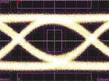
FIGURE 2. An eye diagram of back-to-back transmission depicts performance of a buried tunnel-junction VCSEL at a wavelength of 1.55 µm and direct modulation at 10 Gbit/s.
VCSELs can be directly modulated at up to 10 Gbit/s with wide-open “eye” diagrams (see Fig. 2). An eye diagram is created by overlapping the detected signals for random transmission of zeros and ones. The traces at the center of each bit slot (the center of the eye) should always be above or below a certain threshold to ensure flawless detection. A closed eye indicates inferior performance and increased likelihood of transmission errors.
Vertical-cavity lasers also make ideal sources for trace-gas sensing using tunable laser-diode absorption spectroscopy (see Laser Focus World, November 2004, p. S5). The small volume of the VCSEL cavity leads to significant self-heating due to ohmic losses, shifting the laser wavelength with pumping current by a few nanometers. Using this slight tuning, a fingerprint of the characteristic absorption lines of a gas species can be scanned in a spectroscopy setup.
The concentration can be determined by comparing the recorded spectrum to a database. Such measurements are common in industry (system monitoring, security, sensing of toxic and corrosive gases), as well as in everyday life (environmental measurements, air conditioning).
This method of spectroscopy offers a very short response time compared to conventional sensors-only fractions of a second-which is a key issue for control circuits and security systems. The contact-free remote-sensing capability even admits measurements in corrosive environments. The absorption line strength of most species grows with increasing wavelength, driving the development of VCSELs in this direction to improve system performance.
Materials systems
Short-wavelength VCSELs exploit the well-established gallium arsenide (GaAs)-based aluminum gallium indium arsenide (AlGaInAs) system and use binary AlAs/GaAs DBRs with superb optical and thermal properties. Heat-sinking through these mirrors provides sufficient cooling. Unfortunately, active regions are readily available only up to wavelengths of 1 µm. To reach 1.3 µm, some researchers introduce nitrogen, forming gallium indium arsenide nitride (GaInAsN) quantum wells. This technique is plagued by very sensitive growth conditions but yields devices with the thermal advantages of AlAs/GaAs-based mirrors preserved. These GaInAsN VCSELs reach single-mode output powers of 1.4 mW at room temperature and show good thermal stability. Direct modulation has been demonstrated up to 10 Gbit/s.1
The AlGaInAs material system on an indium phosphide (InP) substrate offers active regions with wavelengths up to 2 µm using strained quantum wells. Unfortunately, the thermal conductivity of InP-based epitaxial DBRs made from ternary and quaternary material drops by more than an order of magnitude as compared to the binary AlAs/GaAs mirrors. Heat-sinking through such a DBR would be insufficient. Therefore, a very thin but highly reflective hybrid dielectric mirror replaces the epitaxial DBR on the backside and enhances heat-sinking. Additionally, a buried tunnel junction allows substitution of most of the p-doped material by n-doped material, leading to lower electrical resistivity. At the same time, this reduces ohmic loss and excess heat generation.
Such devices are available in a wavelength range from 1.3 to 2 µm. A maximum single-mode output power of 1.7 mW at 1.55 µm and room temperature, and operation at over 100°C have already been demonstrated.2 The comparatively relaxed power requirements of only several hundred microwatts for most spectroscopy applications are easily met by these VCSELs, even up to wavelengths of 2 µm.3
To combine the advantages of long-wavelength active regions on InP substrate with the thermal superiority of the GaAs-based DBRs, one approach proposes to grow the constituting components separately on their parent substrates and then “glue” them together by wafer-bonding or fusing. Because of low thermal resistance the devices exhibit excellent characteristics at elevated temperatures, reaching a single-mode output power of 2.1 mW at 1.55 µm and at room temperature. Operation above 90°C has also been demonstrated.4 By adjusting the cavity lengths before fusing, even closely spaced arrays of lasers with a variety of slightly different wavelengths can be manufactured for wavelength-division multiplexing (WDM). While wafer-fused VCSELs can achieve impressive performance, their fabrication technique is rather complicated on full-wafer scale, requiring several epitaxial runs, and reliability is still an issue.
Future research
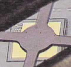
Lasers tunable across dozens of nanometers are desirable components for reconfigurable WDM networks or just as universal spare lasers in case one of the transmitter lasers fails. The tunable laser could be tuned to the required wavelength and take over until the original laser can be replaced. As a result, component storage cost, response times, and downtimes are reduced immensely. A promising concept involves exchanging one of the cavity mirrors of a VCSEL with an electromechanically actuated membrane mirror (see Fig. 3). The bending of the membrane can be adjusted thermally with a heating current or electrostatically, changing the length of the air gap contained in the cavity. The corresponding shift in cavity length and emission wavelength also leads to a change in the output power due to wavelength-dependent laser gain, limiting the tuning range. Recent developments have led to a continuous tuning range of 22 nm around 1.56 µm and a peak output power of 1.3 mW.5 Our group recently increased the tuning range to more than 40 nm using a two-chip concept.6, 7
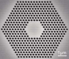
FIGURE 4. In this photonic crystal with a large defect at the center, the etched holes are 300 nm in diameter.
A lot of effort has been placed on the general optimization of existing VCSEL structures, but new concepts have recently drawn interest. Many research groups try to incorporate photonic-crystal structures into their VCSELs (see Fig. 4). The waveguiding properties of photonic crystals can be tailored to support only one transverse mode, thus boosting single-mode output power. Such devices could also be engineered to use optical bistability and serve as optical memory, or as single-photon sources for tap-proof communications.8
Most molecules feature much stronger absorption lines at higher wavelengths, which could potentially result in greatly improved spectroscopy sensitivity or a reduced absorption path. The small, easy-to-handle systems would make hand-held security sensors, which would be of interest to, for example, the mining industry. The aluminum gallium indium arsenide antimonide (AlGaInAsSb) materials system on gallium antimonide (GaSb) substrate is a promising candidate to reach even higher wavelengths, but processing technology is not yet as mature as for InP- and GaAs-based devices. Nonetheless, first results have already been presented.9
Last but not least, there is also potential for surface-emitting devices as light sources for displays. So far, only light-emitting diodes (LEDs) are available for the visible colors red, green, and blue. The materials of choice (II-VI semiconductors, for example), however, pose huge problems with respect to thermal conductivity and lifetime issues. Therefore, VCSELs for these wavelengths with suitable characteristics are not yet expected to appear in the near future.
REFERENCES
1. A. Ramakrishnan et al., Electron. Lett. 38(7) 322 (2002).
2. M. Ortsiefer et al., Electron. Lett. 39(24) 1731 (2003).
3. C. Lauer, M. Ortsiefer, R. Shau et al., IEEE Photon. Technol. Lett. 16(10) 2209 (2004).
4. E. Deichsel, A. Syrbu, A. Caliman et al., Conf. Lasers and Electro-Optics (CLEO) 2004, Postdeadline paper CPDB7 (2004).
5. D Sun, W Fan, P Kner, et al., IEEE Photon. Technol. Lett. 16(3): 714 (2004).
6. M. Maute et al., Electron. Lett. 40(7) 430 (2004).
7. F. Riemenschneider et al., Photon. Tech. Lett. 16, 2212 (2004).
8. M. Dabbicco, T. Maggipinto, M. Brambilla, Appl. Phys. Lett. 86(2) 021116 (2005).
9. A.N. Baranov et al., Electron. Lett. 34(3) 281 (1998).
CHRISTIAN LAUER, MARKUS MAUTE, WERNER HOFMANN, and MARKUS-CHRISTIAN AMANN are all members of the Walter Schottky Institute, Technical University of Munich, Am Coulombwall, 85748 Garching, Germany; e-mail: [email protected].


