Raymond J. Beach and Barry L. Freitas
A laser-diode packaging technology, based on integration that makes it suitable for the construction of large laser-diode arrays, boasts 10- to 100-kW output power capabilities.To imagine 100-kW diode arrays becoming a common reality, two key elements of the technology need to fall into place: high-performance diode bars, and heat sinks that offer excellent thermal management and precision diode-bar mounting. Lawrence Livermore National Laboratory (LLNL; Livermore, CA) has developed a silicon-based packaging technology to solve the challenge of packaging diode bars.
Silicon monolithic microchannels
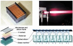
Photolithography and etching techniques are applied to produce thousands of miniscule 30-µm-wide channels in silicon substrates. Water flowing through these microchannels aggressively cools the laser diode bars, which are mounted on the silicon at a location less than 200 µm from the channels (see figure this page). By combining 10 diode bars onto a single heat sink, a 10-bar package (referenced as a tile) serves as the unit cell from which large two-dimensional diode arrays can be built up through tiling.
Individual tiles that make up these large arrays are known as silicon monolithic microchannels (SiMMs; see Fig. 1).1 Considerations that drove the SiMMs package design included ease of fabrication and the ability to construct large laser-diode arrays with 10- to 100-kW output power capabilities. Of paramount importance in the design was the requirement that the same aggressive heat-removal capability that characterized the original rack-and-stack silicon microchannel-cooled package be preserved in the SiMMs (see "Original microchannel-cooled package is still in use," p. 105).2 This challenge was met in the same manner as the original rack-and-stack packageby incorporating microchannels into the silicon directly below the location of the attached laser-diode bars. As in the original rack-and-stack silicon microchannel cooler, the SiMMs design maintains a very tight thermal circuit with only 177 µm of silicon separating the heat-generating laser-diode bars and the microchannel fins that define the cooling channels.
Integrating microlensing attachment technology
Because nearly all applications at Livermore Laboratory now require microlensed arrays, the development of an easy and efficient microlensing attachment technology was an important consideration during the design phase of the SiMMs package. Easy and efficient microlens attachment translated into the requirement that an entire SiMMs package be microlensed in a single step. This eliminates the production steps necessary to individually attach a microlens to each diode bar as we do in our rack-and-stack package. From previous experience with the rack-and-stack package, we knew that microlenses must be placed with a positional tolerance of a few micrometers relative to the diode-bar emitter facets to achieve good optical performance. This implies that the single-step microlensing of an entire SiMMs tile requires the individual diode bars within a tile to be positioned relative to one another with at least the same accuracy.
V-groove technology
The required precision placement of the laser-diode bars on the SiMMs package is accomplished by using V-groove technology on the front surface of the package. V-grooves are generated with the same etching technology used to fabricate the microchannels on the backside of the silicon. In particular, starting with <110> oriented silicon wafers, an etch mask is defined such that the <111> crystallographic planes form etch stops that terminate the etching process and generate the characteristic V-groove contour over the entire surface (see Fig. 2). These V-grooves serve as pads to which the laser-diode bars are registered and attached. V-grooves are defined lithographically, so this technique allows us to locate the output facet of the bars with micrometer precision relative to one another over the entire SiMMs package as required for one-step microlensing.
An unusual feature of the SiMMs package is the 55° angle from the normal at which light is emitted. The emission direction of the diodes at 55° to the normal of the SiMMs front face is due to the orientation of the V-grooves that serve as pads for the laser-diode bars. With the diode bars located, the microlenses can be held in precise frames fabricated in the form of silicon runners in a ladder-like structure consisting of 10 lenses. The entire 10-lens assembly is then attached to the SiMMs package in a single step. This microlens array serves to collimate the fast axis radiation of the laser-diode bars from its original 30° divergence angle into a collimated beam with a divergence angle of less than 1°.
To maintain the aggressive cooling capability of the original rack-and-stack package, microchannels are etched into the backside of the silicon just below the laser-diode bars at their V-groove defined locations. These microchannels etch up into the silicon following the same V-groove contour that characterizes the front of the packagebringing cooling water within 177 µm of the heat-generating diode bars. Microchannels in the SiMMs package are 30 µm wide and located on 60-µm centers. The channels are sourced and drained through a backing glass block that has a manifold structure fabricated into it using glass-milling technology. The backing glass block is attached to the silicon front face using the same anodic bonding technology that is used to join the silicon-glass-silicon laminates in the original rack-and-stack package.
Package performance
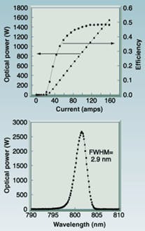
Typical SiMMs package performance generated from a single tile at a 10% duty factor produced a peak optical output power of 1.5 kW (see Fig. 3). This performance was obtained using laser-diode bars with a 1-mm cavity length and 90% fill. The measured thermal resistance of the SiMMs package is 0.32°C/Wth, referenced to a single 1-cm diode bar and the cold inlet water temperature. For example, a diode bar generating 100 Wth of waste heat would experience a 32°C temperature rise at its junction above the temperature of the inlet coolant water.
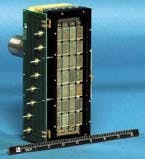
The backing glass blocks of the SiMMs package are designed to sit side-by-side on a backplane structure containing cooling-water source drains. The package is specifically designed for close packing to give high effective fill factors.
Low cost and aggressive thermal performance requirements drove the development of the silicon microchannel approach.4 To understand in more detail how the channels function, it is useful to use a very simplified picture of the heat flow in the structure and break down the temperature rise between the heat-generating laser-diode p-n junction and the cold inlet coolant water into three different components.
The first component corresponds to the temperature rise associated with the heat flowing through the solid silicon material from the laser-diode bar down into the regions between the water flow channels.
The next component corresponds to the temperature rise associated with heat flowing across the stagnant boundary layer of water and into the moving fluid. This stagnant boundary layer exists because of the "no slip" boundary condition at the channel wall-to-wall interface.
The last component corresponds to the temperature rise associated with the heat absorbed by the flowing water as it goes from the cold inlet side of the channel to the hot outlet side of the channel. It turns out that the temperature rise associated with the heat flowing across the stagnant water boundary layer at the solid-to-water interface is generally the largest temperature rise in flowing water heat-sink structures, such as our microchannel cooler. To understand this, consider that the thermal conductivity of water at 0.0061°C/Wth-cm is 250 times less than that of silicon at room temperature. Thus, in compact flowing water heat-sink structures the biggest leverage in controlling the overall temperature rise is generally associated with minimizing the thickness of the stagnant boundary layer. Boundary layer thickness scales with the channel width for the laminar flow conditions used in our coolers, so the solid material used to construct the cooler should be one that permits easy fabrication of narrow channels. This result explains the apparently paradoxical choice of silicon for the solid material in our heat sink over other more obvious materials with higher thermal conductivities, such as copper.
REFERENCES
- J. A. Skidmore et al., Appl. Phys. Lett. 77, 10 (2000).
- R. J. Beach et al., IEEE J. Quant. Elect. 28, 966 (1992).
- D. Tuckerman et al., IEEE Elect. Device Lett. (EDL-2), 126 (1981).
- R. J. Beach et al., Proc. SPIE Photonics West, 2383 (1995).
RAYMOND J. BEACH is the group leader for diode-pumped solid-state lasers, and BARRY L. FREITAS is the group leader for laser diode packaging at the US Department of Energy's Lawrence Livermore National Laboratory, P.O. Box 808, Livermore, CA 94551; e-mail: [email protected].
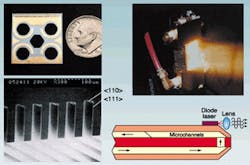
Original microchannel-cooled package is still in useDriven primarily by government applications requiring state-of-the-art lasers, LLNL has maintained a vibrant program focused on the development of high-average-power laser diode arrays since the mid-1980s. The original rack-and-stack silicon microchannel-cooled laser-diode package, developed at LLNL, has been in use since the early 1990s ( see figure).Silicon microchannel-cooled rack-and-stack package relies on narrow water-channel fabrication in silicon to aggressively remove the waste heat generated by laser-diode bars. Top view of the microchannel-cooled package (top left), two-dimensional array illustrates the stacking of individual packages to form a larger multibar array (top right), microchannels (approximately 25 µm wide and 150 µm deep) in silicon fabricated by anisotropic etching (bottom left), and a side view showing the laminated silicon-glass-silicon structure with arrows depicting water flow direction (bottom right) .
This diode package has primarily been used for constructing kilowatt-class arrays consisting of 10 to 50 packages. For this size, the flexibility that stacking brings to building custom arrays has been instrumental to the development of various solid-state lasers constructed at LLNL. However, when scaling to larger arrays, the package does have its disadvantages. Since each package has to be hydraulically sealed to the package next to it, the multiple water seals required in arrays larger than several kilowatts can become a reliability issue. Also, as the price of diode bars continues to drop and their reliability continues to increase, it is advantageous to mount multiple bars on a single microchannel-cooler package to dilute the impact of the cost over many bars rather than just one or two. With these considerations in mind, a second-generation microchannel-cooled package (the SiMMs) has been developed that is capable of holding 10 1-cm bars.


