MARK KEIRSTEAD and PAUL SOMERVILLE
From microlithography to marking and via drilling, ultraviolet (UV) laser applications now represent the fastest-growing segment of the industrial laser market. This growth is due to the unique processing advantages offered by short wavelength laser light, as well as the dramatic maturation of all-solid-state, ultraviolet laser technology.
Disparate needs of the various applications, however, have caused UV laser manufacturers to develop two distinct groups of pulsed laser products—high-repetition-rate (quasi-continuous wave) lasers and high-output-power lasers.
Why UV lasers?
There are some advantages of processing with UV light versus longer wavelengths. Infrared or visible laser light usually processes materials by producing intense local heating that can melt or vaporize the material. Unfortunately, this heating can cause serious damage to surrounding areas limiting both edge strength and the ability to create small, precise features.
In contrast, UV laser light directly breaks the bonds holding a material's atomic constituents together. This atomization is a "cold" process, producing virtually no peripheral heating. This characteristic makes the UV laser an ideal tool for processing delicate materials, such as thin latex and plastics. It also enables the creation of precise marks, holes, or cuts in everything from metals to semiconductors. The ability of UV lasers to perform precision processing is further aided by the fact that the minimum diameter of a focused laser spot is directly proportional to its wavelength (due to diffraction); thus, a shorter wavelength means higher spatial resolution.
For many years, the only sources of UV laser light were gas lasers: excimer lasers for pulsed applications, and ion and helium- cadmium lasers for continuous wave applications. Each of these technologies has significant drawbacks for industrial uses, including a large footprint, limited reliability, high power consumption, and high cost of ownership. In addition, the excimer laser produces a poor quality beam requiring the use of a photomask, which may waste up to 95% or more of the output power. Many helium-cadmium lasers and "low-end" ion lasers also suffer from poor beam pointing stability.
Fortunately, the past decade has seen tremendous advances in diode-pumped, solid-state laser technology. Significant design efforts have been made to optimize the way pump laser output is coupled into the laser crystal, as well as to improve the opto-mechanical design of the laser resonator. The resultant combination of high peak power, excellent mode quality, and high long-term pointing stability has enabled the development of reliable, frequency-tripled lasers offering output around 355 nm.
Progress in diode laser technology has pushed pump laser lifetimes for these products over 10,000 hr. Furthermore, designs that locate the diode pump lasers in the power supply and fiber-couple their output into the laser head vastly simplify the replacement of pump lasers and completely eliminate the need for subsequent optical realignment. This arrangement also makes these laser heads extremely compact (smaller than a shoe box) and doesn't require external water cooling, finally bringing turnkey operational simplicity to UV laser applications.
The majority of commercial, diode-pumped, solid-state lasers utilize Nd:YAG, Nd:YVO4, or Nd:YLF as the gain medium. However, it is the maturation of Nd:YVO4 that has been critical in enabling frequency-tripled lasers to rapidly gain market share. This is because applications for UV lasers fall into two distinct categories: those that require CW (or quasi-CW) performance, and those that require high power. For quasi-CW applications, the high gain and extremely short excited-state lifetime of Nd:YVO4 (neodymium-vanadate) allows it to be operated at very high repetition rates (greater than 100 kHz) with short pulse durations and high peak output power. High peak power insures efficient harmonic generation into the ultraviolet.
Applications in review
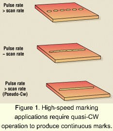
Marking of high-band-gap semiconductors is a typical industrial application that benefits from the use of very-high-repetition rate UV lasers. Quasi-CW operation is essential to produce a continuous mark as the beam is rapidly deflected across the part by high-speed galvanometer mirrors (see Figure 1).
Intergen Inc.,(Sunnyvale, CA) is a supplier of integrated laser marking systems to a number of markets, including the semiconductor industry. According to the firm's president Kris Madeyski, two factors have combined to force the semiconductor industry to switch to marking at shorter wavelengths. "Traditionally," he says, "ink, and more recently, near-infrared lasers were used to mark the plastic encapsulation of chips with unique lot and/or part numbers. But today, the increasing use of technologies such as flip-chip and ball grid arrays (BGA) has created a demand to mark the semiconductor surface itself.
"At the same time, the new high- band-gap materials used for visible LEDs and blue diode lasers are fairly transparent to near-infrared and visible laser light. As a result, near-IR lasers do not produce clean surface marks, but penetrate deep into the wafer, causing microcracking and/or damage to the inner layers."
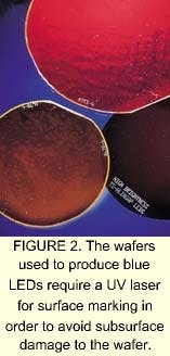
Recently, Intergen was asked to supply marking systems for Hewlett-Packard (now LumiLeds Inc., Mountain View, CA) to mark the AlGaInP wafers used to produce blue LEDs. The goal was to produce a clean surface mark on the gallium-phosphide protective top layer of the wafer. Madeyski explains, "In tests, we found that even green and blue laser light would pass through this transparent window layer and cause microcracking. We therefore designed a system around a high- repetition-rate, diode-pumped Nd:YVO4 laser at 355 nm from Spectra-Physics."
Kyle Thomas of LumiLeds explains the advantages of all- solid-state lasers over gas lasers. "In conjunction with Intergen, we investigated several UV laser sources, including excimer lasers (at 248 nm and 308 nm) and helium-cadmium lasers. The excimer is too big for use in our cleanroom environment. In addition, the poor beam quality of the excimer laser necessitates the use of a photomask for marking. Since we need to mark each wafer uniquely, the mask must be changed between each mark. The HeCd is a little less bulky and produces an acceptable beam for direct writing. Still, we rejected this choice because of size and reliability, as well as the HeCd's need for external water-cooling.
"On the other hand, the diode-pumped, solid-state laser produces a high-quality (TEM00) beam, and also features a very small footprint, turnkey operation, high reliability, and air cooling." These characteristics translate into low cost of ownership, meaning that the wafer marking process adds minimal cost to LED production. This is important when fabricating commodity products such as LEDs" (see Figure 2).Until recently, the excimer laser was the preferred source in most UV materials processing applications because it is easily capable of generating multiple watts of average output power. In these applications, higher power translates directly into greater processing speed and increased production throughput.
Exitech Inc. (Menlo Park, CA) is a builder of laser micromachining systems incorporating infrared, visible, and UV lasers, and also offers contract micromachining services. The company recently began to utilize diode-pumped lasers with 4 W of output power. According to Daffyd Thomas of Exitech, "This laser type has proved effective for a number of tasks in our applications lab, most notably microvia drilling, cutting flex circuits, drilling and cutting polymers, and patterning thin film layers for flat panel displays. For example, when cutting flex circuits we have found that 355-nm laser light virtually eliminates the edge charring that is typical of infrared laser processing."
Microvia drilling is one of the fastest-growing laser application because of the drive for increasing miniaturization in electronic products and consumer goods. But, as Thomas points out, "Via drilling presents several challenges because of the different materials involved. The RF-excited CO2 laser is the preferred tool for drilling the dielectric material, but the light is reflected, rather than absorbed, by the copper layers." In the Exitech system, the diode-pumped UV laser drills through the top layer of 1/2 ounce copper. The CO2 laser is then used to drill through the polymer (up to 125-µm thickness) down to the copper ground plane.
Why choose a high-power UV laser? According to Thomas, "Depending on polymer thickness, a CO2 laser can drill at high speed: up to 60,000 holes/minute. Consequently, the UV laser is the rate-limiting tool. With the 3-W UV laser we formerly used, we could only drill about 1500 holes/min.
"By switching to a 4-W laser, we instantly increased throughput to 2000 holes/min. Any increase in throughput is important when manufacturing commodity products such as electronic packages. Of course, an excimer laser produces much more raw power, but most (up to 95%) of this power is wasted because of masking, so it doesn't deliver the throughput." Exitech has recently licensed its dual-laser technology to Excellon Automation (Los Angeles, CA), because it is very complementary to Excellon's existing line of mechanical drilling stations; these are used to drill macro (>3-mm -diam.) vias.
Solid-state solutions
Diode-pumped solid-state construction is in many ways the ideal laser technology, offering mechanical ruggedness, extremely high reliability, minimal service downtime, and low operating cost. Furthermore, the excellent output characteristics of these lasers especially lend themselves to efficient frequency multiplication. Now, a mature generation of frequency-tripled, diode-pumped, solid-state lasers, using Nd:YVO4 as a gain medium, offer these benefits to a broad range of UV applications, when they require high repetition rate and high peak power operation.
Mark Keirstead and Paul Somerville are with Spectra-Physics, Mountain View, CA (P) 650-961-2550.

