Microvia formation in PCBs
MICHAEL KAUF and HENRY MARTINEZ
The strong market trend to digital and handheld products as well as the convergence of both technologies is pushing microvia production. Devices such as cell phones, pagers, Web browsers, personal digital assistants, digital music players, digital cameras and so on either decrease in size (voice activation) or combine more of the above functions by constant volume (Net access with cell phones). Either way, the printed circuit boards (PCBs) used for these devices are becoming more and more complex.
Mechanical drilling, a proven technology, covers a large range of via diameters down to 200 µm with high aspect depth-to-width ratios. However, a gap remains on the way to microvias. Fortunately, there are special techniques available such as Electric Field Sensing (EFS) for extreme precise blind via formation down to 100 µm to bridge this gap.1 EFS is even available as an upgrade kit and offers an easy way to microvia production using mechanical drilling.
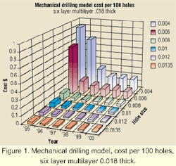
So, why not use EFS for all microvia production? The answer is shown in Figure 1. With declining via diameter the drill bits become more expensive and have to be exchanged more frequently. In summary, the cost per 100 vias is low for large diameters but increases considerably at 150 µm and rises even more for 100 µm. EFS offers a great tool if only a small percentage of microvias are to be manufactured. For large-scale microvia production, laser via formation is more economical and offers a much higher throughput.
Laser processing has already been established for microvia formation and is growing strongly. Worldwide microvia production output nearly doubled from June 1999 to August 2000, with the laser share increased to more than 90 percent.2 CO2 lasers are efficiently used for blind via formation in dielectric materials. With wavelengths between 9.6 µm and 10.6 µm, they are available with high peak and average power, at relatively low cost. However, CO2 lasers show limitations due to their wavelength when drilling copper-clad material or for via sizes of 75 µm and below.
Ultraviolet (UV) lasers can easily produce microvias down to 25 µm, because of their short wavelength. They also can ablate copper and, therefore, overcome the limitation of one layer depth. Industrial diode-pumped, solid-state UV lasers, such as the Coherent (Santa Clara, CA) AVIA series, deliver stable output of more than 3 W average power at 355 nm. This feature combined with an average maintenance cycle of at least 20,000 hours translates to more than three years of two-shift operation. Good beam quality (M2 < 1.3) ensures a minimum focus diameter and maximum depth of focus, resulting in well-defined vias with small taper angle. As more powerful UV lasers become available, the productivity will also improve greatly.
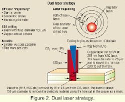
Dual laser systems, such as the Excellon LVD 2001 DP, feature both a solid-state, UV laser and a sealed CO2 laser. These systems combine the "best of both worlds," the UV laser for the most precise and flexible copper ablation followed by the CO2 laser for fast and efficient dielectric removal (see Figure 2). Applying the dual laser strategy, the UV laser is used like a milling tool to ablate the copper surface. Starting at the center of the via, the laser spot (approx. 25 µm) is moved in concentric circles until the desired via diameter is achieved. With declining via diameter this process becomes more and more efficient. The CO2 laser, with a spot size much larger than the actual via size, uses the opening in the copper as a contact mask to ablate the dielectric below. This way, dual laser via formation combines the advantages of high drilling rates (due to the CO2 laser) with minimum via size to 25 µm and high accuracy (due to the UV laser).The dual-laser design is adaptable to different processes and needs. With both UV and CO2 laser capabilities it can be used for CO2 processing, for UV processing or dual laser via formation. Some typical results achieved with dual laser formation follow. All samples were processed with an Excellon LVD 2001 DP with 3 W average UV power and 80 W average CO2 power. There was no desmear or plating applied; the samples were not polished, but only filled with white paint for better contrast of the hole wall angle and the background and examined by cross-sectioning. The drill rates given were measured by drilling test coupons without exceeding the scan field (50 x 50 mm2). For a real board, including skiving and alignment, the drill rate would be lower, depending on the number and distribution of vias per board.
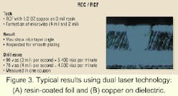
Figure 3 shows a typical microvia in resin-coated copper foil (RCF) with 18-µm copper on 75-µm resin. The microvias have 100-µm diameter and are nicely tapered for easy subsequent plating. In RCF the wall quality is consistent because the resin is homogeneous. Drill rates above 100 vias per second can be achieved.Figure 3 shows a typical microvia of 150-µm diameter in 18-µm copper on top of 63.5-µm dielectric. In this sample the dielectric material is a matrix material with interwoven glass-fibers in resin (FR4-1080). The glass and the resin have different thermodynamic properties, with the glass having the higher transition temperature. The vias produced at given positions statistically hit areas of either low or high fiber content, due to the inhomogeneous interwoven glass structure. Though the laser parameters are absolutely constant, the non-uniformity of the fiber distribution results in higher variation of the via geometry. In Figure 3, there is a high glass fiber content at the right via side and a low content at the left side, causing asymmetry of the via geometry. The drill rate in FR4-1080 was determined to be 65 vias per second or 3,850 vias per minute.
The cost per 1,000 laser vias or the cost per panel, respectively, can be calculated from the throughput of the laser system and the total system costs per hour. They consist of the fixed costs such as depreciation, operator's salary and floor space as well as the hourly operating costs such as consumables, power and water. The dominating share is depreciation, determined by the machine price, followed by the operator's salary.
The costs for consumables are low for state-of-the-art lasers with long component lifetime. For the samples discussed, 4 mil RCF and 6 mil FR4-1080, the costs per 1,000 vias are below $0.50 for 4 mil RCF and below $0.60 for 6 mil FR4-1080 using the Excellon LVD 2001 DP. Comparing the costs of mechanical and laser via formation shows an advantage for the mechanical technology for vias with a diameter of 200 µm. Vias with diameters 150 µm and below are drilled more economically with a laser.
We can now distinguish four scenarios:
- Scenario A puts emphasis on mechanical drilling with the need to manufacture only a few microvias. This can be done economically with EFS on mechanical systems. Even though the manufacturing of the microvias with EFS is a little bit more expensive, the low workload doesn't justify a laser system.
- Scenario B describes via diameters that can be manufactured with mechanical or laser technology. With the laser being more economical and via diameters continuing to decrease, laser via formation is the recommended technology.
- Scenario C puts emphasis on high throughput microvia production. Therefore laser processing is the way to go.
- Scenario D covers the complete spectrum from large vias to microvias. Both, mechanical and laser drilling capabilities will be needed.
There is a strong trend towards dual laser via formation, because this process provides the highest accuracy and smallest via diameters combined with maximum throughput. The best solution depends on the specific situation. We have developed guidelines for certain scenarios to choose the right technology.
REFERENCES
- Lee Ekblad, Michael Kauf, "Knowing the Drill," Printed Circuit Fabrication (PC Fab), June 2000, pp.39-46.
- Brian W. Baird, "Lasers Drive Electronics to the Cutting Edge," Photonics Spectra, December 2000, pg. 86-88
Dr. Michael Kauf is product marketing manager and Henry Martinez is general manager with Excellon Automation Co., Torrance, CA. Contact Mike Kauf at Tel: (310) 534-6363, Fax: (310) 534-6707 or e-mail [email protected].


