Microdisk LEDs light semiconductor display
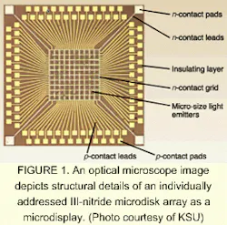
Researchers at Kansas State University (KSU; Manhattan, KS) have fabricated a prototype semiconductor microdisplay based on their previously reported work with arrays of interconnected microdisk light-emitting diodes (LEDs; see Laser Focus World, December 2000, p. 38).1 The blue microdisplay prototype is based on indium gallium nitride/gallium nitride quantum wells and has dimensions of 0.5 x 0.5 mm. It consists of a 10 x 10 array of 12-µm-diameter pixels (see Fig. 1).2
"No one else has fabricated semiconductor microdisplays, which require the integration of a dense array of micro-sized LEDs on a single semiconductor chip," said Jingyu Lin, who is a co-leader of the KSU research group with Hongxing Jiang. Color conversion for full-color displays cannot be achieved in conventional III-V or silicon semiconductors, she explained. Hence, the large, semiconductor-LED, flat-panel displays seen on building facades and stadium scoreboards consist of a massive number of discrete devices.
Current microdisplays are based on liquid-crystal-display (LCD) technology or organic light-emitting diodes (OLEDs), said Lin. But unlike LCDs that normally require external light sources, III-V blue microdisplays are self-luminescent, saving both space and power while enabling viewing from any angle without color shift or degradation in contrast. In addition, to maintain device reliability, OLEDs must be driven at current densities many orders of magnitude lower than semiconductor devices, she said. So they are not yet suitable for the high-power demands of outdoor use. Also, III-nitride devices are grown on sapphire substrates, which are transparent to light and hence provide a natural surface for image display, potentially simplifying device-packaging requirements for large-area-display applications.
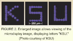
The output wavelength of the KSU devices was on the order of 450 nm and could be varied between 400 and 540 nm by varying the indium content in the active layers of the devices. The researchers plotted output power against input current for three of the microdisk LEDs within the microdisplay, and observed a linear relationship and high output power of about 19 µW for an input current on the order of 6 mA. The speed of these devices was on the order of 0.2 ns. During fabrication, aluminum gallium nitride/gallium nitride was incorporated in the super lattice of the devices, which along with a rapid annealing step more than doubled the hole-mobility of the devices. The p-type concentration achieved was 5 x 1017 cm-3, which is proportional to hole mobility.Since the fabrication of micro-sized LEDs requires much less sophistication than vertical-cavity surface-emitting lasers, the KSU researchers believe that III-nitride, blue-output, micro-sized LED arrays will offer an attractive alternative for inexpensive optical links, said Lin. Despite their small size, the microdisplays can also provide a virtual image comparable to viewing a 21-in.-diagonal television or computer screen when put into an eyeglass headset and viewed through a lens system, she added (see Fig. 2).
REFERENCES
- H. X. Jiang et al., Appl. Phys. Lett. 77, 3236 [Also presented at the Fall 2000 meeting of the Materials Research Society (Nov. 27-Dec. 1; Boston, MA)].
- H. X. Jiang et al., Appl. Phys. Lett. 78, 1303 (Feb. 26, 2001).
About the Author
Hassaun A. Jones-Bey
Senior Editor and Freelance Writer
Hassaun A. Jones-Bey was a senior editor and then freelance writer for Laser Focus World.

