Extreme ultraviolet lithography negotiates remaining obstacles

Increasing the optical power output of the illumination system is the primary focus of the industry and government consortium that hopes to keep pace with Moore's Law by developing the extreme-ultraviolet lithography (EUVL) engineering test stand (ETS), completed last spring at Sandia National Laboratories (Livermore, CA), into a commercially available source of 50-nm printed circuit linewidths by the 2005 to 2006 time frame.
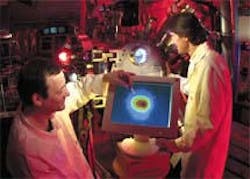
Of two technologies under consideration, the ETS is currently illuminated by a 1500-W Nd:YAG laser provided by TRW (El Segundo, CA), according to Charles Gwyn, general manager for the EUV Corp. and program director for the EUVL program at the Virtual National Laboratory (see figure).
While providing plenty of power for the prototype, the 1500-W Nd:YAG only yields about 10% of the power that will be needed for a production system, Gwyn said. Most of the laser output is dissipated in generating the EUV radiation, and is further reduced by the collection, focusing, and beam-shaping process that ultimately delivers the EUV source illumination to the exposure tool in the form of 13.4-nm soft x-rays.
The process begins with focusing the Nd:YAG beam onto a xenon gas or liquid jet to produce a plasma. Since the soft x-rays produced by the plasma are absorbed by most materials, including the atmosphere, they must be collected, focused, and shaped in a vacuum without the aid of conventional optical materials. "We use mirrors," Gwyn said.
The mirrors are coated with alternating layers of molybdenum and silicon to produce quarter-wave Bragg reflectors and ultimately operate like a conventional optical system, but one that is based on reflective as opposed to transmissive optics. Each mirror is only about 70% efficient, however, so the 10 to 11 mirrors that are required for a production system reduce the flux reaching the wafer to a fraction of that generated by the laser-produced plasma, Gwyn said.
"The source is the biggest remaining challenge, not from the standpoint of being able to produce EUV, but to get the power that we need," he said. "Certainly we have the power with today's sources to support an experimental tool, but as we go forward we need to generate, collect, and focus about 100 W of EUV power into the chamber where the exposures occur."
TRW is working to scale the source upward in terms of output power, and to increase the efficiency of the optical collection and conversion steps. For instance, Gwyn hopes to double the laser-to-EUV conversion efficiency from the current 1/2% to more than 1%. Electrical arc discharges are also being investigated as alternatives to laser power for plasma generation, but the primary focus is on the laser-powered source.
Once the illumination is converted and collected, it enters a main exposure chamber where wafers are exposed by a step-and-scan lithographic process, in which magnetically levitated stages control both the scanning position and velocity within nanometer tolerances. The lithographic masks, as with the system optics, are reflective as opposed to transmissive, and for such fine linewidths they must be produced with defect levels on the order of .003 per square centimeter. A major challenge in this area—although not as much of a challenge as boosting the illumination power—will be improving the multilayer coating tool to meet production demands as well.
"The other major challenge is to transfer the technology to commercial industry so that they can provide the production tools when they are needed," Gwyn said. And the industry partnerships for that stage have already begun.
Industry consortium takes on 10-GHz challenge
Moore's Law, which calls for an order-of-magnitude increase in processing speeds to 10 GHz by 2007, is driving the EUV Corp., which was originated by Intel in 1997 and currently represents an industry consortium consisting of Intel (Santa Clara, CA), AMD (Sunnyvale, CA), Motorola (Schaumburg, IL), Micron (Boise, ID), Infineon (Munchen, Germany) and IBM (Armonk, NY). The Virtual National Laboratory, officially formed in 1997 to work with the EUV Corp. under a Cooperative Research And Development Agreement project, consists of Lawrence Livermore National Laboratory (Livermore, CA), Sandia National Laboratory (Livermore, CA and Albuquerque, NM) and Lawrence Berkeley National Laboratory (Berkeley, CA). The team faces three main challenges in meeting the long-term goal, of which the power requirement is number one.
About the Author
Hassaun A. Jones-Bey
Senior Editor and Freelance Writer
Hassaun A. Jones-Bey was a senior editor and then freelance writer for Laser Focus World.